Fast Electronics for Future Experiments Gary S. Varner University - - PowerPoint PPT Presentation

fast electronics for future experiments
SMART_READER_LITE
LIVE PREVIEW

Fast Electronics for Future Experiments Gary S. Varner University - - PowerPoint PPT Presentation

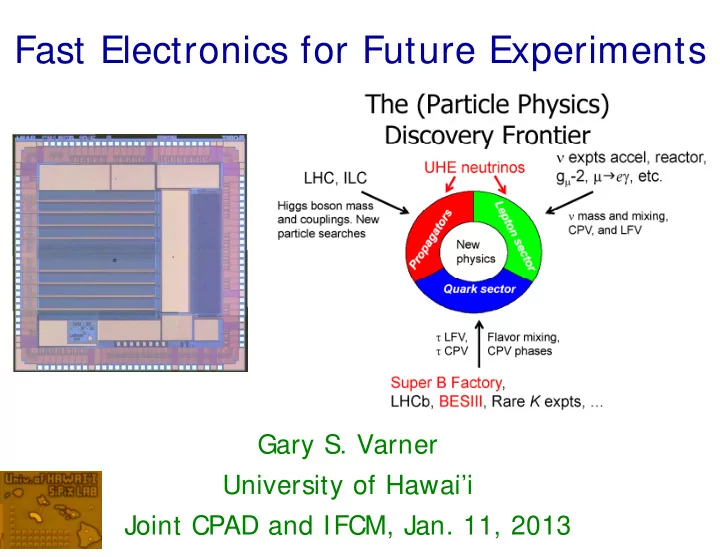
Fast Electronics for Future Experiments Gary S. Varner University of Hawaii University of Hawai i Joint CPAD and IFCM, Jan. 11, 2013 Overview Further advances at the Discovery Frontier Depends upon developing new instruments and


slide-1
SLIDE 1

Fast Electronics for Future Experiments

Gary S. Varner University of Hawai’i University of Hawai i Joint CPAD and IFCM, Jan. 11, 2013

slide-2
SLIDE 2

Overview

  • Further advances at the Discovery Frontier

– Depends upon developing new instruments and techniques – Exploit commodity resources

  • The “easy” experiments are being completed

y p g p

– Can’t necessarily scale up ($$$, T>N*tgradstudent) – Innovation fuels new opportunities Innovation fuels new opportunities

  • What I hope to convey:

1 A “Gi ” E i li f t ti i t ll

  • 1. A new “Giga” Era implies fast timing naturally
  • 2. Introduce key elements

3 A l h hi h b f d ll bli

  • 3. An example where this has been fundamentally enabling
  • 4. A notion toward future directions

2

slide-3
SLIDE 3

History Detector Instrumentation Evolution

  • Traditional “crate based” electronics

– Gated Analog-to-Digital Converters

Det chan

Q-ADC TDC

– Referenced “triggered” Time-to-Digital Converters

Disc. TDC Trigger

  • High-rate applications

– “pipelined operation” – Low-speed, low-resolution sampling

  • High channel counts

– Motivation to reduce cabling – Integrate electronics onto detector elements

Det chan

FADC

Issues: cost, power, resolution, data volume

3

slide-4
SLIDE 4

A “Giga” Overview (Modern Readout)

  • 2. 100’s of Gigaflops per

Field-Programmable Gate Array

  • 4. Commodity Servers

running at Giga-Hz rates, 1000’ f Gi fl

Physical

Gate Array 1000’s of Gigaflops

Physical

Measurement

  • 1. Gigasample/s

“digital oscilloscope

  • 3. Inexpensive Giga-bit/s
  • n a chip”

fiber link interconnect; Giga-bit ethernet

4

Technology advances  high rate, high-precision experiments

slide-5
SLIDE 5

Focus on the first of these

  • 2. 100’s of Gigaflops per

Field-Programmable Gate Array

  • 4. Commodity Servers

running at Giga-Hz rates, 1000’s of Gigaflops

Physical

Gate Array 1000 s of Gigaflops

Physical

Measurement

  • 1. Gigasample/s

“digital oscilloscope

  • 3. Inexpensive Giga-bit/s
  • n a chip”

fiber link interconnect; Giga-bit ethernet

5

  • Defines limit of the physical measurement
  • What Instrumentation Physicists contribute
slide-6
SLIDE 6

Underlying Technology

  • Track and Hold (T/ H)

Analog Input

Sampled Data

T/H C g p

  • Pipelined storage = array of T/ H

l t ith t t b ff i elements, with output buffering

V1=V N capacitors Write Bus Vout=A / (1+A) * Q/Cs =V1 * A/(1+A) Bottom Read Top Read Bus 2

v

V1=V Q=Cs.V 1 1 Bottom Read BUS 4 Cs Return Bus N caps 3

6

slide-7
SLIDE 7

Switched Capacitor Array Sampling

  • Write pointer is ~few

switches closed @ once

Input

s tc es c osed @ o ce

20fF

Input

Tiny charge: 1mV ~ 100e- Channel 1 Channel 2

Few 100ps delay

7

slide-8
SLIDE 8

Basic Functional components

On or off- chip ADC Single storage Ch l chip ADC S l ti i Channel Sample timing Control Few mm x Few mm in size Readout Control

8

slide-9
SLIDE 9

The Giga Package

  • 2 GSa/s, 1GHz ABW

T k i S Tektronics Scope

  • 2.56 GSa/s LAB

WFS ASIC Commercial

S li Sampling speed 0.1-6 GSa/s 2 GSa/s Bits/ENOBs 16/9-13+ 8/7.4

“oscilloscope on

Power/Chan. < = 0.05W Few W

a chip”

Cost/Ch. < $10 (vol) > 100$

9

slide-10
SLIDE 10

Very broad Impact

AMBER Neutrinos LAPPD Fundamental enabling technology (smallest to largest) LAPPD 10

slide-11
SLIDE 11

To be explicit, a demanding Application

~320ps

Measured Measured

~7m

  • RF Transient (impulsive)

Events (200-1200 MHz) 32 h @ 2 6GS /

  • 324 chan. @ 2.6GSa/s
  • Completely solar powered

(tight demands on po e (tight demands on power, few hundred W total)

  • Need full waveforms

A t ti I l i T i t A t

  • Need full waveforms

Antarctic Impulsive Transient Antenna (ANITA-I)

11

slide-12
SLIDE 12

ANITA concept

Typical balloon field of regard

12

Ice RF clarity: Effective “telescope” aperture:

~4km deep ice!

clarity: ~1.2km(!) attenuation p p

  • ~250 km3 sr @ 1018 eV
  • ~104 @ km3 sr 1019 eV

( length (compare to ~1 km3 at lower E)

12

slide-13
SLIDE 13

Large Analog Bandwidth Recorder and Digitizer ith O d d R d t [LABRADOR] with Ordered Readout [LABRADOR]

  • Common

Straight Shot STOP acquisition

  • 3.2 x 2.9 mm
  • Conversion in

RF inputs 120s (all 2340 samples)

  • Data transfer

8+1 chan. * 256+4 samples takes 80s

  • Ready for next

event in 200s

  • Switched

Capacitor Array (SCA)

  • Massively

parallel Wilkinson ADC array Random access:

13

slide-14
SLIDE 14

LABRADOR performance

12-bit ADC 2.6GSa/s

1.3mV

  • 10 real bits (1.3V/1.3mV noise)
  • Excellent linearity, noise
  • Sampling rates up to 4 GSa/s with voltage overdrive

14

slide-15
SLIDE 15

SURFv3 Board

(SURF = Sampling Unit for RF) (TURF = Trigger Unit for RF)

SURFv3 Board

J4 to TURF J1 to CPU LAB3 RF Inputs Programming/ Monitor Header Monitor Header Trigger Inputs

15

PCI bus: 64bits, 66MHz ~ 0.5 GigaByte/s (upgrading for 3rd flight)

slide-16
SLIDE 16

A “high rate” Experiment

Logical segmentation Top cluster (example Trigger Type = 1 shown)

g p

Raw Signals

L2 = 2 of 5 Phi = 0 (1 of 16) Bottom cluster L2 = 2 of 5

Level-1 Level-2 Level-3 Prioritizer

SS

L2 = 2 of 5 Nadir cluster L2 = 2 of 3

Antenna f Cluster 2 f 5 Phi 2 f 2 Prioritizer (+compress)

n TDRS

3-of-8 2-of-5 2-of-2

ents/min

100 200kH Few kHz @ 36kBy/evt = 36-72Mby/s 5-10Hz @ 36kBy/evt = 180-360kBy/s

T di k

Few eve

80 RF channels @ 1.5By * 2.6GSa/s 100-200kHz @ 36kBy/evt = 3.6-7.2Gby/s

To disk

F

= 312 Gbytes/s

Permits thermal noise level operation

16

slide-17
SLIDE 17

17

slide-18
SLIDE 18

The “no free lunch” Theorem

  • Excellent results obtained
  • 1. Made the ANITA project possible & highly successful
  • 2. Similar architectures being studied for new and upgraded

experiments

  • 3. Minimize costs for large systems
  • Not a magic solution

– Significant constraints – Technology in its infancy – will continue to improve

  • Limits and future directions

The technology in a bit more detail The technology, in a bit more detail

18

slide-19
SLIDE 19

Constraint 0: An Intrinsic Limitation

No power (performance savings) for continuous digitization

Won’t displace Flash ADCs

g

“d i ” “down conversion”  For most “triggered” ‘event’ applications, not a serious drawback

19

slide-20
SLIDE 20

Constraint 1: Analog Bandwidth

Difficult to couple in Large BW (C is deadly)

RFamp inside ASIC RFamp inside ASIC

Vin Vsig ZS ZS Ω 50 C in Vin Vsig ZT

f3dB = 1/2ZC

20

slide-21
SLIDE 21

Bandwidth Limitations (LAB1 example)

  • For 1 2GHz C < ~ 2pF (NB input protection diode ~ 10pF)

f3dB = 1/2ZC Would like smallest possible Cstore

  • For 1.2GHz, C < ~ 2pF (NB input protection diode ~ 10pF)
  • Minimize C, (Cdrain not negligible x260)

21

slide-22
SLIDE 22

An Example Bandwidth Evaluation

Transient

9 channels of LAB3

Impulse

9 channels of 256 samples LAB3 To do

FFT Difference

f3dB ~> 1.2GHz

better, reduce

Frequency [GHz]

input and storage C storage C

22

slide-23
SLIDE 23

Constraint 2: kTC Noise

Want small storage C, but…

23

slide-24
SLIDE 24

Similar Constraint 2b: Leakage Current

Increase C or reduce conversion time << 1mV Sample channel-channel variation Sample channel-channel variation ~ fA leakage typically

24

slide-25
SLIDE 25
  • No missing codes

Constraint 3: Digitization

12-bit ADC

  • Linearity as good as

can make ramp

  • Can bracket range of

interest Run count during ramp

Wilki ADC Wilkinson ADC

  • Excellent linearity
  • Basically as good as can make current source/comparator
  • Comparator ~ 0.4 – 2.1V; 133MHz GCC max (~ 31us)

25

slide-26
SLIDE 26

Constraint 4: Sample Aperture Variance

  • Inverter chain has transistor

i ti

  • variations

 ti between samples differ  “Fixed pattern aperture jitter”

  • “Differential temporal nonlinearity”

TDi= ti – tnominal

i i nominal

  • “Integral temporal nonlinearity”

TI i = ti – itnominal

  • “Random aperture jitter” = variation
  • f ti between measurements

t1 t2 t3 t4 t5

i

TD TI TD1 TI 5

26

slide-27
SLIDE 27

Non-uniform sampling timebase

SURF data SURF data

Long-suffering ANITA collaborator Long suffering ANITA collaborator

27

slide-28
SLIDE 28

dT Spread

2.6 GSa/s [LABRADOR3]

10-15% of dT typical

28

slide-29
SLIDE 29

Average aperture calibration

  • Fixed aperature offsets are

Fixed aperature offsets are constant over time, can be measured and corrected

  • Several methods are commonly

used (sine fit [left], zero-crossing)

  • Most use sine wave with random

phase and correct for TDi on a l b statistical basis

29

slide-30
SLIDE 30

Sine Curve Fit Method

i



 

     

500 1024 2 2

min )) ) 2 sin( ( (

j i j i j j j ji

  • f

i a y    

j j

yji : i-th sample of measurement j aj fj j oj : sine wave parameters

j j j j

i : phase error  fixed jitter

“Iterative global fit”: Iterative global fit :

  • Determine rough sine wave parameters

fo each meas ement b fit for each measurement by fit

  • Determine i using all measurements

where sample “i” is near zero crossing

  • Make several iterations
  • S. Lehner, B. Keil, PSI

j

30

slide-31
SLIDE 31

Option 1: Even Faster Sampling p p g

6 GSPS * 8 = 48 GSPS ) 8 = 25ps) (200ps/8 delays

Possible with delay is implemented on PCB

  • b

d ay p d o

31

slide-32
SLIDE 32

Constraint 5: Cross-talk

Coupling between wire-bonds, Vref

32

slide-33
SLIDE 33

Advantage 1: Compact, low-power

  • Comparable performance to best CFD + HPTDC
  • Time difference measurement of recorded pulses
  • Using full samples significantly reduces the impact of
  • Using full samples significantly reduces the impact of

noise

CH1

6.4 ps RMS

CH2

(4.5ps single)

CH2

33

slide-34
SLIDE 34

Advantage 2: Scaling to Large Systems

  • ASIC costing well understood, very competitive!

g , y p

NIM A591 (2008) 534-345.

Storage Depth Capacity

100

Economy of Scale for Quoted ASICs

1000

BLAB ASIC cost estimate

10 100 in [us] at 10GSa/s mpling 4 Chan

100 1000 2007 $]

Based on actual fabrications

  • r quotations from

foundaries

0.1 1 2 4 6 8 10 Storage Depth i Sam 8 Chan 16 Chan 32 Chan

10 per Channel [2

2 4 6 8 10 Array Linear Dimension [mm]

0.1 1 Cost 10 100 1000 10000 100000 1000000 Total Number of System Channels

34

slide-35
SLIDE 35

The Future (?) [A jumping off point…]

ASI C Amplificat # Depth/ ch Sampling Vendo Size Ext ASI C Amplificat ion? # chan Depth/ ch an Sampling [GSa/ s] Vendo r Size [nm] Ext ADC? DRS4 no. 8 1024 1-5 I BM 250 yes. SAM no. 2 1024 1-3 AMS 350 yes. I RS2 no. 8 32536 1-4 TSMC 250 no. BLAB3A yes. 8 32536 1-4 TSMC 250 no. TARGET no 16 4192 1-2 5 TSMC 250 no TARGET no. 16 4192 1-2.5 TSMC 250 no. TARGET2 yes. 16 16384 1-2.5 TSMC 250 no. TARGET3 no. 16 16384 1-2.5 TSMC 250 no. PSEC3 no. 4 256 1-16 I BM 130 no. PSEC4 no. 6 256 1-16 I BM 130 no.

 Success of PSEC: proof-of-concept of moving toward smaller feature sizes.

  • Next DRS plans to use 110nm; next SAM plans to use 180 nm.
slide-36
SLIDE 36

Summary

h The Era Fast Electronics for Electronics for Instrumentation is here

  • Enables whole new

ways of instrumenting detectors

  • Commodity

components and processes open whole new opportunities

36

slide-37
SLIDE 37

Back-up slides p

37

slide-38
SLIDE 38

Simulated Performance vs. SNR

300MHz ABW, 5.9GSa/s

Time Difference Dependence on Signal-Noise Ratio (SNR)

20 16 18 20

  • n [ps]

  kTZ

10 12 14 e Resolutio 4 6 8 e Differenc 2 4 10 100 1000 Tim 10 100 1000 Signal Noise Ratio

38