EE3C11: Structured Electronic Design My First Voltage Ampli fi er - - PowerPoint PPT Presentation

ee3c11 structured electronic design my first voltage
SMART_READER_LITE
LIVE PREVIEW

EE3C11: Structured Electronic Design My First Voltage Ampli fi er - - PowerPoint PPT Presentation

EE3C11: Structured Electronic Design My First Voltage Ampli fi er Design example EE3C11 47u 100n + 5 1k OPA211 Unit step response - 20k 120 27 + - 100 1u 3.4n 2.2p 80 47u 20k 600 1k 220 60 + GAIN 47u 40 - 20 0 -20


slide-1
SLIDE 1

1

(c) 2020 A.J.M. Montagne

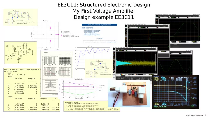
Checking circuit: myFirstVampCompensated.cir No errors found! GAIN DC value = 9.189e+01 Poles: RealPart ImagPart Frequency Q ___________ ___________ __________ _______ p_1

  • 7.8738e+05

7.8738e+05 p_2 -1.6015e+06 1.9166e+06 2.4976e+06 0.77977 p_3

  • 1.6015e+06
  • 1.9166e+06

2.4976e+06 0.77977 p_4 -1.9604e+07 0 1.9604e+07 0 p_5

  • 2.383e+07

2.383e+07 p_6 -5.0504e+08 0 5.0504e+08 0 Zeros: RealPart ImagPart Frequency Q ___________ ___________ __________ _______ z_1 -1.061e+07 0 1.061e+07 0 z_2

  • 3.9963e+07

3.9963e+07 z_3 -8.0941e+08 -7.4266e+08 1.0985e+09 0.67858 z_4

  • 8.0941e+08

7.4266e+08 1.0985e+09 0.67858

+

  • +
  • +
  • 1k

1k 47u 47u 220 20k 2.2p 27 47u 100n 20k 600 3.4n 5 1u OPA211

EE3C11: Structured Electronic Design My First Voltage Amplifier Design example EE3C11

.model OPA211_A0 OV + cd = 8p ; differential-mode input capacitance + gd = 50u ; differential-mode input conductance + cc = 2p ; common-mode input capacitance + av = {A_0*(1+s/2/PI/40M)/(1+s/2/PI/120)/(1+s/2/PI/20M)} ; voltage gain + zo = {3.6k/(1+s*3.6k*8u) + 0.7 + s*900n*60/(60+s*900n)} ; output impedance

0.5 1 1.5 2

time [s]

#10-6

  • 20

20 40 60 80 100 120

Unit step response

GAIN

102 103 104 105 106 107

frequency [Hz]

  • 150
  • 100
  • 50

50 100

magnitude [dB] Magnitude plots

ASYMPTOTIC LOOPGAIN SERVO DIRECT GAIN

slide-2
SLIDE 2

2

(c) 2020 A.J.M. Montagne

Application and initial specification

slide-3
SLIDE 3

3

(c) 2020 A.J.M. Montagne

Application and initial specification ADC

+

slide-4
SLIDE 4

4

(c) 2020 A.J.M. Montagne

Application and initial specification

Signal source: voltage, mean value=0, max. deviation +/- 25mVp

ADC

+

slide-5
SLIDE 5

5

(c) 2020 A.J.M. Montagne

Application and initial specification

Signal source: voltage, mean value=0, max. deviation +/- 25mVp Source impedance: resistive, about 600 Ohm

ADC

+

slide-6
SLIDE 6

6

(c) 2020 A.J.M. Montagne

Application and initial specification

Signal source: voltage, mean value=0, max. deviation +/- 25mVp Source impedance: resistive, about 600 Ohm Load: voltage mean value = 2.5V max. deviation +/- 2.25Vp

ADC

+

slide-7
SLIDE 7

7

(c) 2020 A.J.M. Montagne

Application and initial specification

Signal source: voltage, mean value=0, max. deviation +/- 25mVp Source impedance: resistive, about 600 Ohm Load: voltage mean value = 2.5V max. deviation +/- 2.25Vp Load impedance: capacitive, up to 3.4nF

ADC

+

slide-8
SLIDE 8

8

(c) 2020 A.J.M. Montagne

Application and initial specification

Signal source: voltage, mean value=0, max. deviation +/- 25mVp Source impedance: resistive, about 600 Ohm Load: voltage mean value = 2.5V max. deviation +/- 2.25Vp Load impedance: capacitive, up to 3.4nF Small-signal bandwidth: 100Hz ... 500kHz

ADC

+

slide-9
SLIDE 9

9

(c) 2020 A.J.M. Montagne

Application and initial specification

Signal source: voltage, mean value=0, max. deviation +/- 25mVp Source impedance: resistive, about 600 Ohm Load: voltage mean value = 2.5V max. deviation +/- 2.25Vp Load impedance: capacitive, up to 3.4nF Small-signal bandwidth: 100Hz ... 500kHz Full-power bandwidth: >= 100kHz

ADC

+

slide-10
SLIDE 10

10

(c) 2020 A.J.M. Montagne

Application and initial specification

Signal source: voltage, mean value=0, max. deviation +/- 25mVp Source impedance: resistive, about 600 Ohm Load: voltage mean value = 2.5V max. deviation +/- 2.25Vp Load impedance: capacitive, up to 3.4nF Small-signal bandwidth: 100Hz ... 500kHz Full-power bandwidth: >= 100kHz

ADC

+

  • Noise figure < 3dB
slide-11
SLIDE 11

11

(c) 2020 A.J.M. Montagne

Application and initial specification

Signal source: voltage, mean value=0, max. deviation +/- 25mVp Source impedance: resistive, about 600 Ohm Load: voltage mean value = 2.5V max. deviation +/- 2.25Vp Load impedance: capacitive, up to 3.4nF Small-signal bandwidth: 100Hz ... 500kHz Full-power bandwidth: >= 100kHz Supply voltage: 5V

ADC

+

  • Noise figure < 3dB
slide-12
SLIDE 12

12

(c) 2020 A.J.M. Montagne

Application and initial specification

Signal source: voltage, mean value=0, max. deviation +/- 25mVp Source impedance: resistive, about 600 Ohm Load: voltage mean value = 2.5V max. deviation +/- 2.25Vp Load impedance: capacitive, up to 3.4nF Small-signal bandwidth: 100Hz ... 500kHz Full-power bandwidth: >= 100kHz Supply voltage: 5V Operating temperature: room temperature

ADC

+

  • Noise figure < 3dB
slide-13
SLIDE 13

13

(c) 2020 A.J.M. Montagne

Application and initial specification

Signal source: voltage, mean value=0, max. deviation +/- 25mVp Source impedance: resistive, about 600 Ohm Load: voltage mean value = 2.5V max. deviation +/- 2.25Vp Load impedance: capacitive, up to 3.4nF Small-signal bandwidth: 100Hz ... 500kHz Full-power bandwidth: >= 100kHz Supply voltage: 5V Operating temperature: room temperature

ADC

+

  • Noise figure < 3dB
slide-14
SLIDE 14

14

(c) 2020 A.J.M. Montagne

Engineering characteristics

slide-15
SLIDE 15

15

(c) 2020 A.J.M. Montagne

Engineering characteristics

Amplifier performance requirements

slide-16
SLIDE 16

16

(c) 2020 A.J.M. Montagne

Engineering characteristics

Amplifier performance requirements

P1 Input impedance P3 Load capacitance P2 Input voltage P4 Quiescent load voltage P7 Noise figure @ 600 Ohm P6 Rate of change output voltage P8 Small-signal bandwidth P5 Load signal voltage >> 600 Ohm 50 mVpp 3400 pF 2.5 VDC 4.5 Vpp >=1.41 V/us <= 3 dB 100Hz ... 500kHz P9 Gain and bias inaccuracy <= 3%

slide-17
SLIDE 17

17

(c) 2020 A.J.M. Montagne

Engineering characteristics

Amplifier performance requirements Cost factors

P1 Input impedance P3 Load capacitance P2 Input voltage P4 Quiescent load voltage P7 Noise figure @ 600 Ohm P6 Rate of change output voltage P8 Small-signal bandwidth P5 Load signal voltage >> 600 Ohm 50 mVpp 3400 pF 2.5 VDC 4.5 Vpp >=1.41 V/us <= 3 dB 100Hz ... 500kHz P9 Gain and bias inaccuracy <= 3%

slide-18
SLIDE 18

18

(c) 2020 A.J.M. Montagne

Engineering characteristics

Amplifier performance requirements Cost factors

C1 Power supply voltage P1 Input impedance P3 Load capacitance P2 Input voltage P4 Quiescent load voltage P7 Noise figure @ 600 Ohm P6 Rate of change output voltage P8 Small-signal bandwidth P5 Load signal voltage >> 600 Ohm 50 mVpp 3400 pF 2.5 VDC 4.5 Vpp >=1.41 V/us <= 3 dB 100Hz ... 500kHz 5 VDC P9 Gain and bias inaccuracy <= 3%

slide-19
SLIDE 19

19

(c) 2020 A.J.M. Montagne

Engineering characteristics

Amplifier performance requirements Cost factors Environmental conditions

C1 Power supply voltage P1 Input impedance P3 Load capacitance P2 Input voltage P4 Quiescent load voltage P7 Noise figure @ 600 Ohm P6 Rate of change output voltage P8 Small-signal bandwidth P5 Load signal voltage >> 600 Ohm 50 mVpp 3400 pF 2.5 VDC 4.5 Vpp >=1.41 V/us <= 3 dB 100Hz ... 500kHz 5 VDC P9 Gain and bias inaccuracy <= 3%

slide-20
SLIDE 20

20

(c) 2020 A.J.M. Montagne

Engineering characteristics

Amplifier performance requirements Cost factors Environmental conditions

E1 Operating temperature C1 Power supply voltage P1 Input impedance P3 Load capacitance P2 Input voltage P4 Quiescent load voltage P7 Noise figure @ 600 Ohm P6 Rate of change output voltage P8 Small-signal bandwidth P5 Load signal voltage >> 600 Ohm 50 mVpp 3400 pF 2.5 VDC 4.5 Vpp >=1.41 V/us <= 3 dB 100Hz ... 500kHz 5 VDC 20 deg. Celsius P9 Gain and bias inaccuracy <= 3%

slide-21
SLIDE 21

21

(c) 2020 A.J.M. Montagne

Design of amplifier configuration

slide-22
SLIDE 22

22

(c) 2020 A.J.M. Montagne

Design of amplifier configuration

Voltage transfer independent of source and load impedance.

slide-23
SLIDE 23

23

(c) 2020 A.J.M. Montagne

Design of amplifier configuration

Voltage transfer independent of source and load impedance.

slide-24
SLIDE 24

24

(c) 2020 A.J.M. Montagne

Design of amplifier configuration

+

  • +
  • +
  • +
  • Voltage transfer independent of

source and load impedance.

slide-25
SLIDE 25

25

(c) 2020 A.J.M. Montagne

Design of amplifier configuration

+

  • +
  • +
  • +
  • Voltage transfer independent of

source and load impedance. Amplifier concept for establishing a nonzero value for A only

slide-26
SLIDE 26

26

(c) 2020 A.J.M. Montagne

Design of amplifier configuration

+

  • +
  • +
  • +
  • Voltage transfer independent of

source and load impedance. Amplifier concept for establishing a nonzero value for A only Best performance with nonenergic feedback

slide-27
SLIDE 27

27

(c) 2020 A.J.M. Montagne

Design of amplifier configuration

+

  • +
  • +
  • +
  • Voltage transfer independent of

source and load impedance. Amplifier concept for establishing a nonzero value for A only Best performance with nonenergic feedback

Wide-band transformer expensive

slide-28
SLIDE 28

28

(c) 2020 A.J.M. Montagne

Design of amplifier configuration

+

  • +
  • +
  • +
  • Voltage transfer independent of

source and load impedance. Amplifier concept for establishing a nonzero value for A only Passive feedback configuration Best performance with nonenergic feedback

Wide-band transformer expensive

slide-29
SLIDE 29

29

(c) 2020 A.J.M. Montagne

Design of amplifier configuration

+

  • +
  • +
  • +
  • Voltage transfer independent of

source and load impedance. Amplifier concept for establishing a nonzero value for A only Passive feedback configuration

Feedback network increases noise and power losses of controller

Best performance with nonenergic feedback

Wide-band transformer expensive

slide-30
SLIDE 30

30

(c) 2020 A.J.M. Montagne

Design of amplifier configuration

+

  • +
  • +
  • +
  • +
  • +
  • Voltage transfer independent of

source and load impedance. Amplifier concept for establishing a nonzero value for A only Passive feedback configuration

Feedback network increases noise and power losses of controller

Best performance with nonenergic feedback

Wide-band transformer expensive

slide-31
SLIDE 31

31

(c) 2020 A.J.M. Montagne

Design of amplifier configuration

+

  • +
  • +
  • +
  • +
  • +
  • Voltage transfer independent of

source and load impedance. Amplifier concept for establishing a nonzero value for A only Passive feedback configuration

Feedback network increases noise and power losses of controller

Best performance with nonenergic feedback

Wide-band transformer expensive

Nonzero value for A:

slide-32
SLIDE 32

32

(c) 2020 A.J.M. Montagne

Design of amplifier configuration

+

  • +
  • +
  • +
  • +
  • +
  • Voltage transfer independent of

source and load impedance. Amplifier concept for establishing a nonzero value for A only Passive feedback configuration

Feedback network increases noise and power losses of controller

Best performance with nonenergic feedback

Wide-band transformer expensive

Parallel sensing

Nonzero value for A:

slide-33
SLIDE 33

33

(c) 2020 A.J.M. Montagne

Design of amplifier configuration

+

  • +
  • +
  • +
  • +
  • +
  • Voltage transfer independent of

source and load impedance. Amplifier concept for establishing a nonzero value for A only Passive feedback configuration

Feedback network increases noise and power losses of controller

Best performance with nonenergic feedback

Wide-band transformer expensive

Parallel sensing

Nonzero value for A:

Zero output impedance

slide-34
SLIDE 34

34

(c) 2020 A.J.M. Montagne

Design of amplifier configuration

+

  • +
  • +
  • +
  • +
  • +
  • Voltage transfer independent of

source and load impedance. Amplifier concept for establishing a nonzero value for A only Passive feedback configuration

Feedback network increases noise and power losses of controller

Best performance with nonenergic feedback

Wide-band transformer expensive

Parallel sensing Series comparison

Nonzero value for A:

Zero output impedance

slide-35
SLIDE 35

35

(c) 2020 A.J.M. Montagne

Design of amplifier configuration

+

  • +
  • +
  • +
  • +
  • +
  • Voltage transfer independent of

source and load impedance. Amplifier concept for establishing a nonzero value for A only Passive feedback configuration

Feedback network increases noise and power losses of controller

Best performance with nonenergic feedback

Wide-band transformer expensive

Parallel sensing Series comparison

Nonzero value for A:

Infinite input impedance Zero output impedance

slide-36
SLIDE 36

36

(c) 2020 A.J.M. Montagne

Design of amplifier configuration

+

  • +
  • +
  • +
  • +
  • +
  • Voltage transfer independent of

source and load impedance. Amplifier concept for establishing a nonzero value for A only Passive feedback configuration

Feedback network increases noise and power losses of controller

Best performance with nonenergic feedback

Wide-band transformer expensive

Parallel sensing Series comparison

Nonzero value for A:

Infinite input impedance Zero output impedance

slide-37
SLIDE 37

37

(c) 2020 A.J.M. Montagne

Noise design

slide-38
SLIDE 38

38

(c) 2020 A.J.M. Montagne

Noise design

Find and solve design equations for elements that contribute to the noise

slide-39
SLIDE 39

39

(c) 2020 A.J.M. Montagne

Noise design

Find and solve design equations for elements that contribute to the noise

  • 1. Feedback resistors
slide-40
SLIDE 40

40

(c) 2020 A.J.M. Montagne

Noise design

Find and solve design equations for elements that contribute to the noise

  • 1. Feedback resistors
  • 2. Controller equivalent intput noise sources
slide-41
SLIDE 41

41

(c) 2020 A.J.M. Montagne

Noise design

Find and solve design equations for elements that contribute to the noise

  • 1. Feedback resistors
  • 2. Controller equivalent intput noise sources

Noise model:

slide-42
SLIDE 42

42

(c) 2020 A.J.M. Montagne

Noise design

Find and solve design equations for elements that contribute to the noise

  • 1. Feedback resistors
  • 2. Controller equivalent intput noise sources

Noise model:

+

  • +
slide-43
SLIDE 43

43

(c) 2020 A.J.M. Montagne

Noise design

Find and solve design equations for elements that contribute to the noise

  • 1. Feedback resistors
  • 2. Controller equivalent intput noise sources

Noise model:

+

  • +
slide-44
SLIDE 44

44

(c) 2020 A.J.M. Montagne

Noise design

Find and solve design equations for elements that contribute to the noise

  • 1. Feedback resistors
  • 2. Controller equivalent intput noise sources

Noise model:

+

  • +
  • Noise figure of 3dB:
slide-45
SLIDE 45

45

(c) 2020 A.J.M. Montagne

Noise design

Find and solve design equations for elements that contribute to the noise

  • 1. Feedback resistors
  • 2. Controller equivalent intput noise sources

Noise model:

+

  • +
  • Noise figure of 3dB:
slide-46
SLIDE 46

46

(c) 2020 A.J.M. Montagne

Noise design

Find and solve design equations for elements that contribute to the noise

  • 1. Feedback resistors
  • 2. Controller equivalent intput noise sources

Noise model:

+

  • +
  • Noise figure of 3dB:

Show stopper values:

slide-47
SLIDE 47

47

(c) 2020 A.J.M. Montagne

Noise design

Find and solve design equations for elements that contribute to the noise

  • 1. Feedback resistors
  • 2. Controller equivalent intput noise sources

Noise model:

+

  • +
  • Noise figure of 3dB:

Show stopper values:

slide-48
SLIDE 48

48

(c) 2020 A.J.M. Montagne

Noise design

Find and solve design equations for elements that contribute to the noise

  • 1. Feedback resistors
  • 2. Controller equivalent intput noise sources

Noise model:

+

  • +
  • Noise figure of 3dB:

Show stopper values:

slide-49
SLIDE 49

49

(c) 2020 A.J.M. Montagne

Noise design

Find and solve design equations for elements that contribute to the noise

  • 1. Feedback resistors
  • 2. Controller equivalent intput noise sources

Noise model:

+

  • +
  • Noise figure of 3dB:

Show stopper values:

slide-50
SLIDE 50

50

(c) 2020 A.J.M. Montagne

Noise design

Find and solve design equations for elements that contribute to the noise

  • 1. Feedback resistors
  • 2. Controller equivalent intput noise sources

Noise model:

+

  • +
  • Noise figure of 3dB:

Show stopper values:

slide-51
SLIDE 51

51

(c) 2020 A.J.M. Montagne

Voltage and current drive capability

slide-52
SLIDE 52

52

(c) 2020 A.J.M. Montagne

Voltage and current drive capability Load drive requirements

slide-53
SLIDE 53

53

(c) 2020 A.J.M. Montagne

Voltage and current drive capability

Load signal voltage: 4.5Vpp

Load drive requirements

slide-54
SLIDE 54

54

(c) 2020 A.J.M. Montagne

Voltage and current drive capability

Load signal voltage: 4.5Vpp Maximum rate of change @ 100kHz sine wave, 4.5Vpp: 1.41 V/us

Load drive requirements

slide-55
SLIDE 55

55

(c) 2020 A.J.M. Montagne

Voltage and current drive capability

Load signal voltage: 4.5Vpp Maximum rate of change @ 100kHz sine wave, 4.5Vpp: 1.41 V/us Maximum load current @ 100kHz sine wave, 4.5Vpp, 3.4nF: 4.8mA

Load drive requirements

slide-56
SLIDE 56

56

(c) 2020 A.J.M. Montagne

Voltage and current drive capability

Load signal voltage: 4.5Vpp Maximum rate of change @ 100kHz sine wave, 4.5Vpp: 1.41 V/us Maximum load current @ 100kHz sine wave, 4.5Vpp, 3.4nF: 4.8mA

Load drive requirements

Quiescent output voltage: 2.5V

slide-57
SLIDE 57

57

(c) 2020 A.J.M. Montagne

Voltage and current drive capability

Load signal voltage: 4.5Vpp Maximum rate of change @ 100kHz sine wave, 4.5Vpp: 1.41 V/us Maximum load current @ 100kHz sine wave, 4.5Vpp, 3.4nF: 4.8mA

Load drive requirements Supply requirements

Quiescent output voltage: 2.5V

slide-58
SLIDE 58

58

(c) 2020 A.J.M. Montagne

Voltage and current drive capability

Load signal voltage: 4.5Vpp Maximum rate of change @ 100kHz sine wave, 4.5Vpp: 1.41 V/us Maximum load current @ 100kHz sine wave, 4.5Vpp, 3.4nF: 4.8mA

Load drive requirements Supply requirements

Supply voltage: 5V Quiescent output voltage: 2.5V

slide-59
SLIDE 59

59

(c) 2020 A.J.M. Montagne

Voltage and current drive capability

Load signal voltage: 4.5Vpp Maximum rate of change @ 100kHz sine wave, 4.5Vpp: 1.41 V/us Maximum load current @ 100kHz sine wave, 4.5Vpp, 3.4nF: 4.8mA

Load drive requirements Supply requirements

Supply voltage: 5V No power consumption requirements Quiescent output voltage: 2.5V

slide-60
SLIDE 60

60

(c) 2020 A.J.M. Montagne

Voltage and current drive capability

Load signal voltage: 4.5Vpp Maximum rate of change @ 100kHz sine wave, 4.5Vpp: 1.41 V/us Maximum load current @ 100kHz sine wave, 4.5Vpp, 3.4nF: 4.8mA

Biasing errors take a part of the budget for the total voltage drop Load drive requirements Supply requirements

Supply voltage: 5V No power consumption requirements Quiescent output voltage: 2.5V

slide-61
SLIDE 61

61

(c) 2020 A.J.M. Montagne

Voltage and current drive capability

Load signal voltage: 4.5Vpp Maximum rate of change @ 100kHz sine wave, 4.5Vpp: 1.41 V/us Maximum load current @ 100kHz sine wave, 4.5Vpp, 3.4nF: 4.8mA

Biasing errors take a part of the budget for the total voltage drop

Biasing concept with AC coupling

Load drive requirements Supply requirements

Supply voltage: 5V No power consumption requirements Quiescent output voltage: 2.5V

slide-62
SLIDE 62

62

(c) 2020 A.J.M. Montagne

Voltage and current drive capability

Load signal voltage: 4.5Vpp Maximum rate of change @ 100kHz sine wave, 4.5Vpp: 1.41 V/us Maximum load current @ 100kHz sine wave, 4.5Vpp, 3.4nF: 4.8mA

Biasing errors take a part of the budget for the total voltage drop

Biasing concept with AC coupling As presented in Chapter 9

Load drive requirements Supply requirements

Supply voltage: 5V No power consumption requirements Quiescent output voltage: 2.5V

slide-63
SLIDE 63

63

(c) 2020 A.J.M. Montagne

Voltage and current drive capability

Load signal voltage: 4.5Vpp Maximum rate of change @ 100kHz sine wave, 4.5Vpp: 1.41 V/us Maximum load current @ 100kHz sine wave, 4.5Vpp, 3.4nF: 4.8mA

Biasing errors take a part of the budget for the total voltage drop

Biasing concept with AC coupling As presented in Chapter 9

Load drive requirements Supply requirements

Supply voltage: 5V No power consumption requirements Quiescent output voltage: 2.5V

OpAmp requirements

slide-64
SLIDE 64

64

(c) 2020 A.J.M. Montagne

Voltage and current drive capability

Load signal voltage: 4.5Vpp Maximum rate of change @ 100kHz sine wave, 4.5Vpp: 1.41 V/us Maximum load current @ 100kHz sine wave, 4.5Vpp, 3.4nF: 4.8mA

Biasing errors take a part of the budget for the total voltage drop

Biasing concept with AC coupling As presented in Chapter 9

Load drive requirements Supply requirements

Supply voltage: 5V No power consumption requirements

+

  • +
  • Sourcing output saturation

Sinking output saturation Minimum CM input to positive supply Minimum CM input to negative supply CM input voltage range

+

  • {

Quiescent output voltage: 2.5V

OpAmp requirements

slide-65
SLIDE 65

65

(c) 2020 A.J.M. Montagne

Voltage and current drive capability

Load signal voltage: 4.5Vpp Supply voltage: 5V Maximum rate of change @ 100kHz sine wave, 4.5Vpp: 1.41 V/us Maximum load current @ 100kHz sine wave, 4.5Vpp, 3.4nF: 4.8mA

Biasing errors take a part of the budget for the total voltage drop

Biasing concept with AC coupling As presented in Chapter 9

Load drive requirements Supply requirements

Supply voltage: 5V No power consumption requirements

+

  • +
  • Sourcing output saturation

Sinking output saturation Minimum CM input to positive supply Minimum CM input to negative supply CM input voltage range

+

  • {

Quiescent output voltage: 2.5V

OpAmp requirements

slide-66
SLIDE 66

66

(c) 2020 A.J.M. Montagne

Voltage and current drive capability

Load signal voltage: 4.5Vpp Supply voltage: 5V Maximum rate of change @ 100kHz sine wave, 4.5Vpp: 1.41 V/us Maximum load current @ 100kHz sine wave, 4.5Vpp, 3.4nF: 4.8mA

Biasing errors take a part of the budget for the total voltage drop

Biasing concept with AC coupling As presented in Chapter 9

Load drive requirements Supply requirements

Supply voltage: 5V No power consumption requirements

+

  • +
  • Sourcing output saturation

Sinking output saturation Minimum CM input to positive supply Minimum CM input to negative supply CM input voltage range

+

  • {

Quiescent output voltage: 2.5V

OpAmp requirements

Current drive capability: > 4.8mA + current through feedback network

slide-67
SLIDE 67

67

(c) 2020 A.J.M. Montagne

Voltage and current drive capability

Output saturation source/sink: < 0.25V - total output biasing error voltage Load signal voltage: 4.5Vpp Supply voltage: 5V Maximum rate of change @ 100kHz sine wave, 4.5Vpp: 1.41 V/us Maximum load current @ 100kHz sine wave, 4.5Vpp, 3.4nF: 4.8mA

Biasing errors take a part of the budget for the total voltage drop

Biasing concept with AC coupling As presented in Chapter 9

Load drive requirements Supply requirements

Supply voltage: 5V No power consumption requirements

+

  • +
  • Sourcing output saturation

Sinking output saturation Minimum CM input to positive supply Minimum CM input to negative supply CM input voltage range

+

  • {

Quiescent output voltage: 2.5V

OpAmp requirements

Current drive capability: > 4.8mA + current through feedback network

slide-68
SLIDE 68

68

(c) 2020 A.J.M. Montagne

Voltage and current drive capability

Output saturation source/sink: < 0.25V - total output biasing error voltage Load signal voltage: 4.5Vpp Supply voltage: 5V Maximum rate of change @ 100kHz sine wave, 4.5Vpp: 1.41 V/us Maximum load current @ 100kHz sine wave, 4.5Vpp, 3.4nF: 4.8mA

Biasing errors take a part of the budget for the total voltage drop

Biasing concept with AC coupling As presented in Chapter 9

Load drive requirements Supply requirements

Supply voltage: 5V No power consumption requirements

+

  • +
  • Sourcing output saturation

Sinking output saturation Minimum CM input to positive supply Minimum CM input to negative supply CM input voltage range

+

  • {

Quiescent output voltage: 2.5V

OpAmp requirements

Current drive capability: > 4.8mA + current through feedback network

slide-69
SLIDE 69

69

(c) 2020 A.J.M. Montagne

Biasing errors

slide-70
SLIDE 70

70

(c) 2020 A.J.M. Montagne

Biasing errors

+

  • +
  • +
slide-71
SLIDE 71

71

(c) 2020 A.J.M. Montagne

Biasing errors

+

  • +
  • +
  • Contributions to biasing errors:
slide-72
SLIDE 72

72

(c) 2020 A.J.M. Montagne

Biasing errors

+

  • +
  • +
  • Contributions to biasing errors:
  • Supply voltage tolerance
slide-73
SLIDE 73

73

(c) 2020 A.J.M. Montagne

Biasing errors

+

  • +
  • +
  • Contributions to biasing errors:
  • Supply voltage tolerance
  • Resistor tolerances
slide-74
SLIDE 74

74

(c) 2020 A.J.M. Montagne

Biasing errors

+

  • +
  • +
  • Contributions to biasing errors:
  • Supply voltage tolerance
  • Resistor tolerances
  • Bias current OpAmp
slide-75
SLIDE 75

75

(c) 2020 A.J.M. Montagne

Biasing errors

+

  • +
  • +
  • Contributions to biasing errors:
  • Supply voltage tolerance
  • Resistor tolerances
  • Bias current OpAmp
  • Offset current OpAmp
slide-76
SLIDE 76

76

(c) 2020 A.J.M. Montagne

Biasing errors

+

  • +
  • +
  • Contributions to biasing errors:
  • Supply voltage tolerance
  • Resistor tolerances
  • Bias current OpAmp
  • Offset current OpAmp
  • Offset voltage OpAmp
slide-77
SLIDE 77

77

(c) 2020 A.J.M. Montagne

Biasing errors

+

  • +
  • +
  • Contributions to biasing errors:
  • Supply voltage tolerance
  • Resistor tolerances
  • Bias current OpAmp
  • Offset current OpAmp
  • Offset voltage OpAmp

Interaction with other performance aspects:

slide-78
SLIDE 78

78

(c) 2020 A.J.M. Montagne

Biasing errors

+

  • +
  • +
  • Contributions to biasing errors:
  • Supply voltage tolerance
  • Resistor tolerances
  • Bias current OpAmp
  • Offset current OpAmp
  • Offset voltage OpAmp

Interaction with other performance aspects:

  • Noise:
slide-79
SLIDE 79

79

(c) 2020 A.J.M. Montagne

Biasing errors

+

  • +
  • +
  • Contributions to biasing errors:
  • Supply voltage tolerance
  • Resistor tolerances
  • Bias current OpAmp
  • Offset current OpAmp
  • Offset voltage OpAmp

Interaction with other performance aspects:

  • Noise:
  • Bandwidth:
slide-80
SLIDE 80

80

(c) 2020 A.J.M. Montagne

Biasing errors

+

  • +
  • +
  • Contributions to biasing errors:
  • Supply voltage tolerance
  • Resistor tolerances
  • Bias current OpAmp
  • Offset current OpAmp
  • Offset voltage OpAmp

Interaction with other performance aspects:

  • Noise:
  • Bandwidth:
  • Accuracy:
slide-81
SLIDE 81

81

(c) 2020 A.J.M. Montagne

Biasing errors

+

  • +
  • +
  • Contributions to biasing errors:
  • Supply voltage tolerance
  • Resistor tolerances
  • Bias current OpAmp
  • Offset current OpAmp
  • Offset voltage OpAmp

Interaction with other performance aspects:

  • Noise:
  • Bandwidth:
  • Accuracy:
  • PSRR:
slide-82
SLIDE 82

82

(c) 2020 A.J.M. Montagne

Biasing errors

+

  • +
  • +
  • Contributions to biasing errors:
  • Supply voltage tolerance
  • Resistor tolerances
  • Bias current OpAmp
  • Offset current OpAmp
  • Offset voltage OpAmp

Interaction with other performance aspects:

  • Noise:
  • Bandwidth:
  • Accuracy:
  • PSRR:
slide-83
SLIDE 83

83

(c) 2020 A.J.M. Montagne

Biasing errors

(1) (2) (3) (out) (4) X1 O_dcVar

+

  • R3

R4 V1 R2 R1

slide-84
SLIDE 84

84

(c) 2020 A.J.M. Montagne

Biasing errors

(1) (2) (3) (out) (4) X1 O_dcVar

+

  • R3

R4 V1 R2 R1

Simplified result:

slide-85
SLIDE 85

85

(c) 2020 A.J.M. Montagne

Biasing errors

(1) (2) (3) (out) (4) X1 O_dcVar

+

  • R3

R4 V1 R2 R1

Simplified result:

slide-86
SLIDE 86

86

(c) 2020 A.J.M. Montagne

Biasing errors

(1) (2) (3) (out) (4) X1 O_dcVar

+

  • R3

R4 V1 R2 R1

Simplified result:

slide-87
SLIDE 87

87

(c) 2020 A.J.M. Montagne

Bandwidth design

slide-88
SLIDE 88

88

(c) 2020 A.J.M. Montagne

Bandwidth design

Determination of the required GB product of the OpAmp

slide-89
SLIDE 89

89

(c) 2020 A.J.M. Montagne

Bandwidth design

Determination of the required GB product of the OpAmp

Use the simplest model that provides this information:

slide-90
SLIDE 90

90

(c) 2020 A.J.M. Montagne

Bandwidth design

Determination of the required GB product of the OpAmp

Use the simplest model that provides this information: +

slide-91
SLIDE 91

91

(c) 2020 A.J.M. Montagne

Bandwidth design

Determination of the required GB product of the OpAmp

Use the simplest model that provides this information: +

  • +
  • +
slide-92
SLIDE 92

92

(c) 2020 A.J.M. Montagne

Bandwidth design

Determination of the required GB product of the OpAmp

Use the simplest model that provides this information: +

  • +
  • +
slide-93
SLIDE 93

93

(c) 2020 A.J.M. Montagne

Bandwidth design

slide-94
SLIDE 94

94

(c) 2020 A.J.M. Montagne

Bandwidth design

Evaluation of loop gain-poles product

slide-95
SLIDE 95

95

(c) 2020 A.J.M. Montagne

Bandwidth design

Evaluation of loop gain-poles product

+

  • +
  • +
  • +
slide-96
SLIDE 96

96

(c) 2020 A.J.M. Montagne

Bandwidth design

Evaluation of loop gain-poles product

+

  • +
  • +
  • +
slide-97
SLIDE 97

97

(c) 2020 A.J.M. Montagne

Bandwidth design

Evaluation of loop gain-poles product

+

  • +
  • +
  • +
slide-98
SLIDE 98

98

(c) 2020 A.J.M. Montagne

Bandwidth design

Evaluation of loop gain-poles product

+

  • +
  • +
  • +
  • Achievable bandwidth B equals LP product:
slide-99
SLIDE 99

99

(c) 2020 A.J.M. Montagne

Bandwidth design

Evaluation of loop gain-poles product

+

  • +
  • +
  • +
  • Achievable bandwidth B equals LP product:
slide-100
SLIDE 100

100

(c) 2020 A.J.M. Montagne

Bandwidth design

Evaluation of loop gain-poles product

+

  • +
  • +
  • +
  • Achievable bandwidth B equals LP product:
slide-101
SLIDE 101

101

(c) 2020 A.J.M. Montagne

Bandwidth design

Evaluation of loop gain-poles product

+

  • +
  • +
  • +
  • Achievable bandwidth B equals LP product: