Designing Logic Gates Low Swing Signals Note: The tree is reduced - - PowerPoint PPT Presentation

designing logic gates
SMART_READER_LITE
LIVE PREVIEW

Designing Logic Gates Low Swing Signals Note: The tree is reduced - - PowerPoint PPT Presentation

Advanced Digital IC-Design Content Logic Families Designing Logic Gates Low Swing Signals Note: The tree is reduced CMOS Logic Families Static v.s. Dynamic CMOS Design CMOS Logic Families Static - Each gate output have a low Non Clocked


slide-1
SLIDE 1

1

Advanced Digital IC-Design

Designing Logic Gates

Content

Logic Families Low Swing Signals
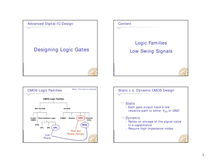
CMOS Logic Families

CMOS Logic Families

Note: The tree is reduced

Non Clocked Clocked Compl. CMOS Pass-transistor Logic C2MOS Domino

TSPC

Clocked CVSL

DCSL

CVSL SPL

CPL

DPL

DCSL

Fast but Power Hungry Low Power

Static v.s. Dynamic CMOS Design Static

  • Each gate output have a low

resistive path to either VDD or GND

Dynamic

  • Relies on storage of the signal value

i it in a capacitance

  • Require high impedance nodes
slide-2
SLIDE 2

2

Static v.s. Dynamic CMOS Design

VDD VDD

fNAND

A B CLK CLK

VDD

fNAND

A B

VDD

fNAND

A B A B

GND GND GND

Static Dynamic

Characteristics

R l ti l l

Static NAND

VDD

Relatively low power In stand-by, only leakage Medium performance Low perf. for large fan-in

fNAND A A B B

High noise margin

  • Low impedance to supply

GND

Ratioed Logic have Resistive Load VDD

OH DD

V V R =

Asymmetrical VTC

t = 0 69 R C

f

PDN

Rpull-up

eq n OL DD eq n pull up

R V V R R

− − −

= +

tpLH = 0.69 Rpull-up CL GND

PDN

Static current when PDN is on

Ratioed Logic Rpull-up >> Ron-n

Depletion mode VT < 0, i.e. always on Static current when PDN is on VDD VDD VDD

R i i NMOS P d

f

GND

DD

PDN

Rpull-up

f

GND

DD

PDN

"Rpull-up"

f

GND

DD

PDN

"Rpull-up"

Static Logic: 2n Transistors Ratioed Logic: n+ 1 Transistors Resistive load NMOS Pseudo- NMOS

slide-3
SLIDE 3

3

Differential Cascode Voltage Switch Logic (DCVSL)

Cross-coupled transistors

No static power

(except leakage)

Fully differential

VDD

PDN

VDD

PDN

A&A

f f

Two dual NMOS PDN nets

GND

PDN

GND

PDN

Dual

B&B

Pass-Transistor Logic

N transistors

Switching

f

No static power consumption in pass transistors

(except leakage)

Switching Network

A B B

f f

AND NAND

A B

f

Pass-transistor Logic

AND/ NAND

B B 1 B f A B

NAND

f

AND

f 1 1 1 B A B

NAND

f

AND

f 1 1 B B B B A B

NAND

f

AND

f 1 1 1 1 A B

NAND

f

AND

f B B

NMOS switch net

VDD Static

DD

B V → The PMOS will not be completely closed while the NMOS is open

  • Static power

X Static Current VX = VDD -VT

DD DD

A V =

V (V)

consumption

VX = VDD -VT

B

V (V)

slide-4
SLIDE 4

4

NMOS Switch Net: Improvement

Level restorer

Advantage: Full Swing Disadvantage: More Complex, Larger Capacitance

X V V

1 B → 1 A =

mr

Careful design: kmr small to be able to sink node X

VX = VDD

1 A =

Careful dimensioning of the

Single Pass-transistor Logic – Level Restorer

g m r transistor

B->VDD mr

Hard to pull

A = VDD B VDD X VX = VDD

Hard to pull down if m r is to strong

Transmission Gate

VDD

B →

A = VDD X

V

VX = VDD

B Symbol 1 B → t

Resistance in a Transmission Gate

R

Req high when VGS close to GND Req high when VGS close to VDD

VIN VOUT

GND

VDD

R

eq n

R

− eq p

R

Vin (V)

eq total

R

slide-5
SLIDE 5

5

Complementary Pass-transistor Logic

(CPL)

Switching Network

Inputs

f

f A f A f A B B B B B B

Inverse Switching Network

f

Inverse Inputs

f AND/NAND f B B A f OR/NOR f B B A f EXOR/XNOR f A A A

C2MOS Clocked Static CMOS

A B

Two Clock Phases Tri-state

  • High impedance output is possible

φ φ No Static Power

B A

Dynamic Logic

VDD VDD

Out PDN In

φ φ

CL

φ φ

PDN In Out

CL

PUN

NMOS Net

GND

φ

GND

φ

PMOS Net Example

n + 2 Transistors

2 i St ti CMOS

VDD

φ

  • 2n in Static CMOS

VOH= VDD and VOL= GND

  • High impedance node at VOH

No Static Power Requires Clock

A

φ

CL

C B

C AB

f

+

Requires Clock

GND

φ

slide-6
SLIDE 6

6

Domino Logic

φ

PDN

φ

PDN

φ

PDN

φ φ φ

All inputs are set to 0 during precharge

Domino Logic - Characteristics

Only non-inverting logic - limits the use Nodes pre-charged only to be discharged

  • high activity

φ φ

PDN

φ φ

PDN

φ φ

PDN

CMOS Logic Families

CMOS Logic Families

CPL is often claimed to be ” The Low Power Family”

Non Clocked Clocked Compl. CMOS Pass-transistor Logic C2MOS Domino

TSPC

Clocked CVSL

DCSL

CVSL SPL

CPL

DPL

DCSL

Low Power ?

CPL vs. CMOS

”CPL: The Low Power Family?”

+ Fewer transistors + Mostly NMOS

  • Need level restorer
  • More wires

smaller transistors

+ Lower internal swing + No input inverters + Smaller stack height + Complex functions with

B A A B F

p a minimum of transistors

A A F

XOR

slide-7
SLIDE 7

7

CPL – XOR Gate

A= 0, B= 0 A= 0, B= 1

B A A B F B A A B F

1 1 1 1 1 1

A A F A A F

1 1 1 1

CPL vs. CMOS – XOR Gate

B B

CPL

VDD

Static CMOS

A A A F F A B

VDD

Q A B A B

6 NMOS 2 PMOS

A

5 NMOS 5 PMOS

CPL: Fast Level Restoring

Cross coupling give fast restoring Lower Power Consumption

B A A B F

Low short-circuit current in inverters

XOR

A A F

CPL Example: Adder - Carry Part Low Stacking Small Transistors

B A A

Small Transistors Lower Power Carry

B B A C C C C C Co A A A

VDD

Co C A A A B

VDD

slide-8
SLIDE 8

8

CPL Example: Adder - Sum Part

The nets are shared Minimum number of transistors Lower Power

A C

Sum

A A A C C C S B B

Sum

B B S C A

CPL Example: Adder with Low Stacking Carry

C B A A A

A A C C S B

Sum

O l 2

B B A Co C C C Co A A A A

VDD VDD

A

VDD VDD VDD

D "0" P

B B A S C C A B

Only 2 stacked

B

C B A B A A B B C C C C A A B B B S Co C A B A

G "1" P

CPL: However! Most reports are on adders Adders and MUXes suites CPL Other circuitry might not show that good result good result

  • R. Zimmerman, JSSC, July 97

Differential Current Switch Logic

Cross-coupled inverters for fast switching (compare to sense amplifiers) Phase 1: Low CLK – Output is precharged

Q Cross-coupled inverters CLK CLK Q

Phase 1: Low CLK Output is precharged 1 1

CLK CLK CLK

NMOS Three NMOS Three

slide-9
SLIDE 9

9

Differential Current Switch Logic

Phase 2: High CLK If Q falls faster Right NMOS three is cut of No Charge up of the right NMOS three

Q Cross-coupled inverters CLK CLK Q

No Charge up of the right NMOS three Low Power

Cut of by Q

CLK CLK CLK

NMOS Three NMOS Three

Conclusions: Logic families

TSPC is fast but power hungry Static CMOS has rather low power cons. CPL and DCSL are known to be better

Low Swing Signals

For long wires (large CL) Can be used locally (e.g. Pass transistors) Conversion between supply voltage regions is needed Restoring/ amplifying circuitry to convert back to high voltage

Low Swing Signals: Idea

Convert to low swing Restore to High swing BUS with high load Local Block Local Block Low swing signals will save power Delays can be reduced using repeaters

slide-10
SLIDE 10

10

Low Swing Driver

NMOS transistor VDD close when the

  • utput voltage reach

VDD-VT Only one supply is Only one supply is needed Low at 0 High at VDD-VT

Low Swing Driver

Up Low Swing Driver (ULD) Down Low Swing Driver (DLD) UDLD Driver (ULD) Driver (DLD)

VDD VDD VDD Low at 0 High at VDD-VT Low at VT High at VDD Low at VT High at VDD-VT

Low Swing Driver

Up Low Swing Driver (ULD) Down Low Swing Driver (DLD)

VDD VDD Low at 0 High at VDD-2VT Low at 2VT High at VDD

Full Swing Receiver

The cross-coupled transistors are restoring the voltage g g Two Supplies are needed VDDhigh High Output Sving Voltage 1 Low Input Sving Voltage VDDlow Sving Voltage 1

slide-11
SLIDE 11

11

Full Swing Receiver

High input

  • M1 turns off
  • M2 turns on
  • M3 turns on

3

  • M4 turns off
  • = > Low output

Low input

  • M1 turns on
  • M2 turns off
  • M turns on

VDD Low swing in High swing out M1 M3 M4

  • M4 turns on
  • M3 turns off
  • = > High output
  • Only one supply

is needed

swing in M2

Full Swing Receiver

Up Down Full swing Receiver (UDFR)

VDD

UFR ( )

Low swing in High swing out VDD VDD High swing out Low swing in Low swing in High swing out

DFR

Repeaters to Reduce the Bus Delay

Up Low Swing Repeater (ULR) Down Low Swing Repeater (DLR) UDLR Repeater (ULR) Repeater (DLR)

VDD VDD VDD

Repeaters to Reduce the Bus Delay

Consider a 20 mm long wire, 1 um wide

R = 2 kΩ C = 20 pF

Buffer data

R = 200 Ω Req 200 Ω Cout = 0.1 pF Cin = 0.1 pF

slide-12
SLIDE 12

12

Repeaters: Buffers Neglected

R 12

0.69 0.69 2000 20 10 27.6 ns RC

× = × × × =

R/2 C/2 R/2 C/2 C 12

0.69 2 0.69 2 1000 10 10 13.8 ns 2 2 R C

× × = × × × × =

R/3 C/3 R/3 C/3 R/3 C/3

0.69 3 9.2 ns 3 3 R C × × =

Repeaters: Buffers included

Cout Cin Cin Cout

1 R n + C 1 R n + C

0.69 ( 1)( ( 1) ) ( ( 1)( )) ( 1) ( 1)

eq

  • ut

in

R C n n R n C C n n × + + + × × + + + + +

n = number of repeaters

Cout Cin Cin Cout

1 n + 1 n +

Buffer data

  • 12

0.69 3 ( 3 ) ( 3 ( )) 3 3 2000 20 0.69 3 ( 3 200) ( 3 0.2) 10 19.1 3 3

eq

  • ut

in

R C R C C ns × × + × + × + = = × × + × × + × × =

Example: n = 2

Buffer data Req = 200 Ω Cout = 0.1 pF Cin = 0.1 pF

Repeaters: Minimum delay

30 35

Minimum delay ith t t

tp (ns)

10 15 20 25 30

Buffers included with two repeaters

1 2 3 4 5 5

Number of repeaters

Buffers excluded