
SLIDE 1
S2, 2008 COMP9032 1
Logic Gates and Typical Functional Blocks
Lecturer: Dr. Annie Guo
S2, 2008 COMP9032 2
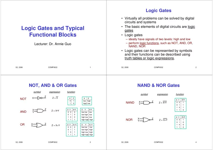
Logic Gates
- Virtually all problems can be solved by digital
circuits and systems
- The basic elements of digital circuits are logic
gates
- Logic gates
– ideally have signals of two levels: high and low – perform logic functions, such as NOT, AND, OR, NAND, NOR
- Logic gates can be represented by symbols
and their functions can be described using truth tables or logic expressions.
S2, 2008 COMP9032 3
NOT, AND & OR Gates
NOT AND OR
X Z = X symbol function X Y Z = X•Y X Y Z = X+Y
X Z 0 1 1 0 X Y X•Y 0 0 0 0 1 0 1 0 0 1 1 1 X Y X+Y 0 0 0 0 1 1 1 0 1 1 1 1 X Z low high high low X Y X•Y low low low low high low high low low high high high X Y X+Y low low low low high high high low high high high high
expression Z Z Z
S2, 2008 COMP9032 4
NAND & NOR Gates
NAND NOR
symbol function X Y Z = X•Y
X Y X•Y 0 0 1 0 1 1 1 0 1 1 1 0 X Y X+Y 0 0 1 0 1 0 1 0 0 1 1 0
X Y Z = X+Y expression Z Z