
1
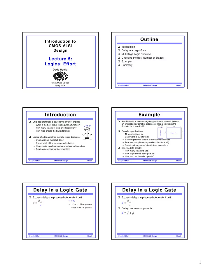
Introduction to CMOS VLSI Design
Lecture 5: Logical Effort
David Harris
Harvey Mudd College Spring 2004
5: Logical Effort Slide 2 CMOS VLSI Design
Outline
Introduction Delay in a Logic Gate Multistage Logic Networks Choosing the Best Number of Stages Example Summary
5: Logical Effort Slide 3 CMOS VLSI Design
Introduction
- Chip designers face a bewildering array of choices
– What is the best circuit topology for a function? – How many stages of logic give least delay? – How wide should the transistors be?
- Logical effort is a method to make these decisions
– Uses a simple model of delay – Allows back-of-the-envelope calculations – Helps make rapid comparisons between alternatives – Emphasizes remarkable symmetries
? ? ?
5: Logical Effort Slide 4 CMOS VLSI Design
Example
- Ben Bitdiddle is the memory designer for the Motoroil 68W86,
an embedded automotive processor. Help Ben design the decoder for a register file.
- Decoder specifications:
– 16 word register file – Each word is 32 bits wide – Each bit presents load of 3 unit-sized transistors – True and complementary address inputs A[3:0] – Each input may drive 10 unit-sized transistors
- Ben needs to decide:
– How many stages to use? – How large should each gate be? – How fast can decoder operate?
A[3:0] A[3:0] 16 32 bits 16 words
4:16 Decoder Register File
5: Logical Effort Slide 5 CMOS VLSI Design
Delay in a Logic Gate
Express delays in process-independent unit
abs
d d τ =
τ = 3RC ≈ 12 ps in 180 nm process 40 ps in 0.6 µm process
5: Logical Effort Slide 6 CMOS VLSI Design
Delay in a Logic Gate
Express delays in process-independent unit Delay has two components
abs