Design of SiC MOSFET Gate Driver Circuit and Development of SiC - - PDF document

design of sic mosfet gate driver circuit and development
SMART_READER_LITE
LIVE PREVIEW

Design of SiC MOSFET Gate Driver Circuit and Development of SiC - - PDF document

Design of SiC MOSFET Gate Driver Circuit and Development of SiC MOSFET Based Buck Converter Archana Manuel 1 and Dr. Dinesh Gopinath 2 1 P. G Student, Rajiv Gandhi Institute of Technology, Mahatma Gandhi University, Kottayam.


slide-1
SLIDE 1

Design of SiC MOSFET Gate Driver Circuit and Development of SiC MOSFET Based Buck Converter

Archana Manuel1 and Dr. Dinesh Gopinath2

  • 1P. G Student, Rajiv Gandhi Institute of Technology, Mahatma Gandhi University, Kottayam.

archanamanuel@gmail.com, Mobile: 9496128256

  • 2Asst. Professor, Rajiv Gandhi Institute of Technology, Mahatma Gandhi University, Kottayam.

Abstract - From small voltage regulators to large motor drives, power electronics play a very important role in present day technology. The power electronics market is currently dominated by silicon based

  • devices. However due to inherent limitations of silicon

material they are approaching thermal limit in terms

  • f high

power and high temperature operation. Performance can only be improved with the development of new power devices with better material properties. Silicon Carbide devices are now gaining popularity as next generation semiconductor

  • devices. Due to its inherent material properties such as

high breakdown field, wide band gap, high electron saturation velocity, and high thermal conductivity, they serve as a better alternative to the silicon

  • counterparts. Here an attempt is made to study the

unique properties of SiC MOSFET and requirements for designing a gate drive circuit for the same. A driver circuit is designed for SiC MOSFET SCH2080KE and its performance is tested by implementing a buck converter. Also the switching characteristics of SCH2080KE is analyzed using LTspice by performing double pulse test.

  • I. INTRODUCTION

Power Electronics play an important role in present day

  • technology. They cover lot of areas including industry,

transportation, utility system, space technology etc. In developed countries it is estimated that around 60% of electrical energy goes through some kind of power electronic converter before its final usage. The present power electronics market is dominated by silicon based devices. However they are approaching their thermal limit, due to its inherent limitations in material characteristics such as

  • 1. Narrow Band gap
  • 2. Low thermal conductivity
  • 3. Low breakdown voltage.

Hence Silicon (Si) based power devices are inadequate to meet the growing needs, especially in high voltage, high efficiency and high power applications. For instance: Si IGBT can handle a voltage up to 5000V but due to its bipolar nature, its switching frequency is limited to 100 kHz. Si MOSFET can handle switching frequency

  • f several MHz, but due to its high ON state resistance the

use of MOSFET is restricted to low voltage application. Also operation of Si based power device is restricted to

  • 1500C. It's the time to turn our focus on devices with

better material characteristics.

  • II. CHARACTERISTICS OF SIC MOSFETS

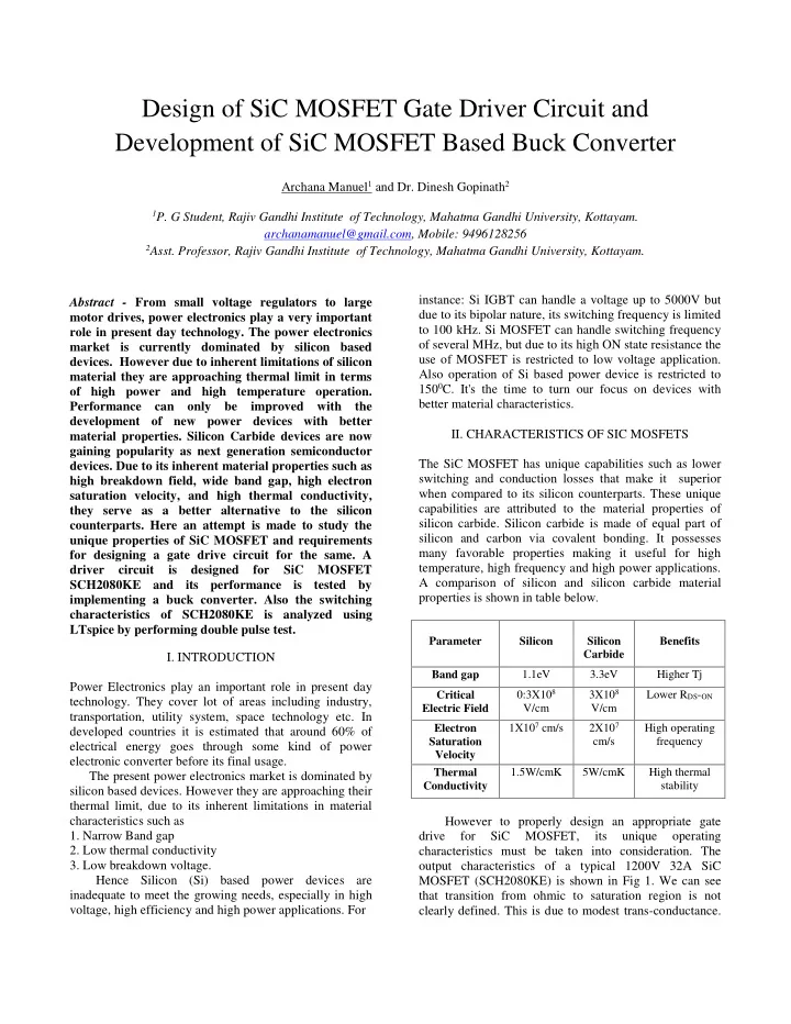
The SiC MOSFET has unique capabilities such as lower switching and conduction losses that make it superior when compared to its silicon counterparts. These unique capabilities are attributed to the material properties of silicon carbide. Silicon carbide is made of equal part of silicon and carbon via covalent bonding. It possesses many favorable properties making it useful for high temperature, high frequency and high power applications. A comparison of silicon and silicon carbide material properties is shown in table below.

Parameter Silicon Silicon Carbide Benefits Band gap 1.1eV 3.3eV Higher Tj Critical Electric Field 0:3X10⁸ V/cm 3X10⁸ V/cm Lower RDS-ON Electron Saturation Velocity 1X107 cm/s 2X107 cm/s High operating frequency Thermal Conductivity 1.5W/cmK 5W/cmK High thermal stability

However to properly design an appropriate gate drive for SiC MOSFET, its unique

  • perating

characteristics must be taken into consideration. The

  • utput characteristics of a typical 1200V 32A SiC

MOSFET (SCH2080KE) is shown in Fig 1. We can see that transition from ohmic to saturation region is not clearly defined. This is due to modest trans-conductance.

slide-2
SLIDE 2

This characteristic plays a vital role while designing fault protection circuits (especially DESAT protection) as drain to source voltage does not increase much with fault current.

Figure 1. Typical SiC MOSFET output characteristics

Another feature of SiC MOSFET is the dependence

  • f RDS on gate to source voltage. Although SiC-

MOSFETs have lower drift layer resistance than Si- MOSFETs, the lower carrier mobility in SiC means their channel resistance is higher. For this reason, the higher the gate voltage, the lower the on-resistance. Resistance becomes progressively saturated as VGS gets higher than

  • 20V. SiC-MOSFETs do not exhibit low on-resistance

with the gate voltage VGS of 10 to 15V.

Figure 2 RDS Vs VGS characteristics of SCH2080KE

  • III. DESIGN OF SiC MOSFET GATE DRIVE CIRCUIT

AND BUCK CONVERTER Driving a SiC MOSFET differs slightly from that of conventional silicon MOSFET or IGBT. Requirements of gate driver circuit are as follows [4]:

  • 1. Needs to be driven with a higher gate voltage swing

than Si MOSFET (+ 20V to -2V / -5V).

  • 2. Negative gate voltage must not go below -5V. Negative

driving voltage is not mandatory and is suggested only when drain current is high (>50A).

  • 4. External gate resistance must be appropriately selected

for minimizing or eliminating ringing in gate drive circuit.

  • 5. Parasitic must be minimized. So gate driver must be

located as close as possible to the gate.

  • 6. It is recommended to connect a 10k between gate and

source to prevent excessive floating of gate during propagation delay. The gate drive circuits for MOSFETs can be of two types: isolated and non-isolated gate drivers. In this driver circuit an optically isolated driver IC TLP250 is used. Peak output current of the driver selected must be high enough, so that it can meet the peak gate current requirements of MOSFET. The peak gate current (Ig) depends on the rate of rise of gate charge (Qg).

= =

= 1.28A

Figure 3. Gate Drive Circuit for SiC MOSFET

We can select the driver IC TLP250 with a peak

  • utput current of 1.5 A. Also supply voltage can vary

from 10  35V hence suitable for providing large gate voltage swing. And it can supports high frequency

  • peration of MOSFET. The driver circuit using TLP250

is shown in Figure 3. Zener diodes are provided to limit the gate to source voltage. Here a voltage swing of 0 – 18V is given to gate as a minimum of 18V is required to completely turn ON MOSFET. Also negative voltage must not go below -5V. Hence ratings of zener are 18V and 3.3V. In this we are implementing a buck converter with SiC MOSFET as switch, to test the performance of gate driver circuit. The output requirements are 10V, 1A. The circuit diagram is shown in Figure 4. The voltage and current requirements of buck converter are Vin min = 15V, Vin max = 24V, V0 =10V, fs =15kHz, I0 = 1A Value of Inductor is given as,

L0 =

slide-3
SLIDE 3

Let the maximum ripple current be 20% of output current, so 2mH inductor is can be selected. Value of output capacitor is given as, C0 =

∆ ∆

Let the ripple voltage be 1% of output voltage. Then 22µF

  • utput capacitor is required. A 10Ω , 10W resistor can be

used as load.

  • IV. SIMULATION STUDY

A buck converter with silicon carbide MOSFET (SCH2080KE) as switch was simulated with designed

  • values. The simulations were carried out in power

electronics design software LTspice IV. Simulated voltage and current waveforms are shown in following figures. Double pulse test was carried out to access the switching performance of SiC MOSFET. Figure 7 illustrates circuit setup for double pulse test. Applied voltage was set to 600 V and current at 10A at the first turn-off and second turn-on switching periods. The turn off occurs at around 15µs and turn on around 20µs. Turn on losses was found to be 244.76µJ and turn

  • ff losses 77µJ. So switching losses at 15 kHz will be

4.82W. Turn ON and turn OFF switching waveforms are plotted in Figure 8. Top plot shows the power loss and bottom plot shows turn ON & turn OFF voltage and current variation. Following table shows a comparison of switching losses at 320C and 1250C. For SiC MOSFET, with the increase

  • f temperature turn on loss decreases and turn off loss
  • increases. As a result there is only a small change in

switching loss as temperature increases. Current Turn OFF Losses(µJ) Turn ON Losses(µJ) 320C 1250C 320C 1250C 10A 12.32 14.48 26.048 24.51 20A 31.238 59.89 91.823 86.203 30A 71.44 115.42 168.07 151.79

Figure 4 Buck Converter with SiC MOSFET switch Figure 5 Output of Buck Converter Figure 6 Current through and voltage across inductor Figure 7 Circuit Diagram of Double Pulse Test Figure 8 Switching Characteristics of SCH2080KE

slide-4
SLIDE 4
  • V. HARDWARE RESULTS

A gate drive card using TLP250 driver IC with a voltage swing of 18V (0 to 18V) is implemented. Its performance is tested using a buck converter. The switching pulses of amplitude 5V and frequency 15 kHz is given as the input to diver IC from function generator. A 24V DC is given to the buck converter from a regulated voltage supply. The output wave forms are measured using a digital signal oscilloscope (DSO).

Figure 10 Buck Converter and Gate Drive Card Figure 11 Output of Gate Driver IC

Following table shows the variation of ON state voltage drop with gate to source voltage. In this drain to source voltage is kept a constant and gate to source voltage is varied from 14V to 18V. The On state voltage drop is noted for each gate to source voltage. The on state voltage drop corresponds to the on state drain to source resistance. We can see that the drop is least for 18V. Vgs ON - state Voltage drop 14V 35mV 15.2V 30mV 16V 15.8mV 17.3V 13mV 18V 11mV

  • V. CONCLUSION

This paper makes an attempt to study the switching characteristics of SiC MOSFET and gate drive consideration for the same. An open loop buck converter with SiC MOSFET as switch is also designed. Driving a SiC MOSFET is easy. Conventionally available MOSFET

  • r IGBT driver ICs can be used for this purpose. The

difference lies in the input gate voltage swing required. The advisable voltage swing is from -5V to 22V. From the analysis of variation of on state voltage drop with gate to source voltage we can understand that when gate to source voltage is 18V the on state voltage drop is

  • minimum. That is unlike silicon MOSFET, a gate voltage
  • f 15V does not give a minimum ON state resistance for

SiC MOSFETs. This explains the need for higher voltage

  • swing. One of the disadvantages of silicon carbide

MOSFET is that it is expensive. This may be solved in future. REFERENCES [1] "Silicon Carbide power devices and modules" Rohm semiconductor application note, June 2013. [2] Hangseok Choi "Overview of silicon carbide power devices" Fairchild semiconductor application note. [3] Sam Davis "1200V SiC MOSFET Poised to Replace Si MOSFETs and IGBTs" Power Electronic Technology, pp.36-40, February 2011. [4] Julius Rice,John MookKen "Silicon carbide MOSFET gate drive design consideration" IEEE ,pp.24-27, January 2015. [5] P. Friedrichs. “SiC power devices for industrial applications,” Power Electronics Conference (IPEC), 2010 International, 2010, pp. 3241-3248.

Figure 9 Experimental Setup Figure 12 Output of Buck Converter