Clk strobing PO[y] PO[x] PO[0] Clk 2 Capture Row FFs HELP - - PowerPoint PPT Presentation

clk strobing
SMART_READER_LITE
LIVE PREVIEW

Clk strobing PO[y] PO[x] PO[0] Clk 2 Capture Row FFs HELP - - PowerPoint PPT Presentation

HOST HELP Details ECE 525 Hardware-Embedded Delay PUF (HELP) Details Challenge Clk 1 Launch Row FFs PI[y] PI[x] PI[0] Clk 1 Clk 2 Functional Unit Clk strobing PO[y] PO[x] PO[0] Clk 2 Capture Row FFs HELP integrates into the


slide-1
SLIDE 1

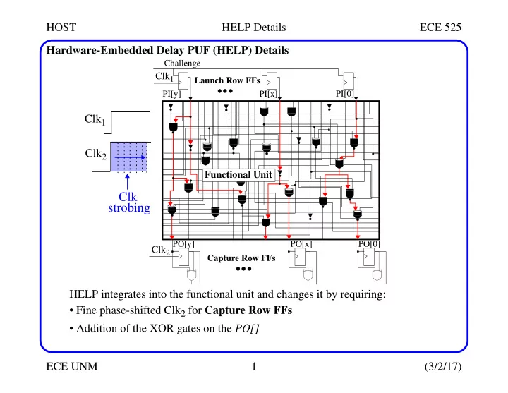
HOST HELP Details ECE 525 ECE UNM 1 (3/2/17) Hardware-Embedded Delay PUF (HELP) Details HELP integrates into the functional unit and changes it by requiring:

  • Fine phase-shifted Clk2 for Capture Row FFs
  • Addition of the XOR gates on the PO[]

Clk1 Clk2

Clk strobing

Clk1

PI[0] PI[y] PI[x] Challenge Launch Row FFs Capture Row FFs

Clk2

PO[0] PO[x] PO[y]

Functional Unit

slide-2
SLIDE 2

HOST HELP Details ECE 525 ECE UNM 2 (3/2/17) PUF Number (PN) Generation 1) C program running under linux gets 2-vector sequences from Host (secure server) 2-vector sequences represent the Challenges which are transferred across the GPIO interface to the PL side

  • 1st vector of the sequence is stored in the Launch1 FFs
  • GPIO FFs are used to store 2nd vector

C program starts the Launch-Capture (LC) Test Engine

Clk1

PI[0] PI[y] PI[x] Challenge Launch Row FFs Capture Row FFs

Clk2

PO[0] PO[x] PO[y]

Functional Unit

Launch1

GPIO Arm µP

PS side PL side

DDR RAM RAM disk 512 MB AXI NIC

Host ethernet

Launch2

GPIO Evaluation Module FPA Mod. MMCM LC Test Driver 2 1 3 init LC Mod. 4 Linux OS 5 8 PN Trans. 7 done eval init 6 inc

slide-3
SLIDE 3

HOST HELP Details ECE 525 ECE UNM 3 (3/2/17) PUF Number (PN) Generation 2) Launch-Capture (LC) Test Driver set initial phase to 1 between Clk1 and Clk2 The MMCM has digital controls which allows the phase shift to be incremented

  • r decremented in steps (each take about 12 clk cycles) of size 17.86 ps

3) LC Test Driver starts Evaluation Module to carry out initialization (zero’s out a set

  • f registers)

This completes initialization for this vector sequence (this is repeated for the subsequent vector sequences)

Clk1

PI[0] PI[y] PI[x] Challenge Launch Row FFs Capture Row FFs

Clk2

PO[0] PO[x] PO[y]

Launch1

GPIO Arm µP

PS side PL side

DDR RAM RAM disk 512 MB AXI NIC

Host ethernet

Launch2

GPIO Evaluation Module FPA Mod. MMCM LC Test Driver 2 1 3 init LC Mod. 4 Linux OS 5 8 PN Trans. 7 done eval init 6 inc

Functional Unit

slide-4
SLIDE 4

HOST HELP Details ECE 525 ECE UNM 4 (3/2/17) PUF Number (PN) Generation 4) LC Test Driver starts the LC Module which selects the 2nd vector values on the mux On the next rising edge of Clk1, transitions will propagate through the Func- tional Unit as highlighted in red With the phase shift set to 1 initially, the XOR gates (which store the 1st vector values) generate ’1’ for paths that have actual transitions and ’0’ otherwise

Clk1

PI[0] PI[y] PI[x] Challenge Launch Row FFs Capture Row FFs

Clk2

PO[0] PO[x] PO[y]

Functional Unit

Launch1

GPIO Arm µP

PS side PL side

DDR RAM RAM disk 512 MB AXI NIC

Host ethernet

Launch2

GPIO Evaluation Module FPA Mod. MMCM LC Test Driver 2 1 3 init LC Mod. 4 Linux OS 5 8 PN Trans. 7 done eval

Clk1 Clk2 Initial phase shift is small ’1’ ’0’

init 6 inc

slide-5
SLIDE 5

HOST HELP Details ECE 525 ECE UNM 5 (3/2/17) PUF Number (PN) Generation 5) LC Test Driver starts the Evaluation Module which analyzes the XOR outputs The 11-bit timing registers (not shown but inside the Evaluation Module) are set to the current phase shift for PO[]s with XOR outputs equal to ’1’ 6) LC Test Driver starts FPA Module to increment the phase shift As long as at least on XOR gate remains at ’1’, steps 4), 5) are 6) are repeated

Clk1

PI[0] PI[y] PI[x] Challenge Launch Row FFs Capture Row FFs

Clk2

PO[0] PO[x] PO[y]

Functional Unit

Launch1

GPIO Arm µP

PS side PL side

DDR RAM RAM disk 512 MB AXI NIC

Host ethernet

Launch2

GPIO Evaluation Module FPA Mod. MMCM LC Test Driver 2 1 3 init LC Mod. 4 Linux OS 5 8 PN Trans. 7 done eval

Clk1 Clk2 Subsequent phase shifts are larger ’1’ ’0’

init 6 inc

slide-6
SLIDE 6

HOST HELP Details ECE 525 ECE UNM 6 (3/2/17) PUF Number (PN) Generation 7) LC Test Driver returns to idle when all XOR outputs become zero and asserts done to the C program (which is busy waiting on this signal) 8) The C program starts PN Trans to obtain (one at a time) and store the n-bit timing values If additional 2-vector sequences are to be applied, the C program loads the next vec- tor sequence (step 1) and the whole process is repeated

Clk1

PI[0] PI[y] PI[x] Challenge Launch Row FFs Capture Row FFs

Clk2

PO[0] PO[x] PO[y]

Launch1

GPIO Arm µP

PS side PL side

DDR RAM RAM disk 512 MB AXI NIC

Host ethernet

Launch2

GPIO Evaluation Module FPA Mod. MMCM LC Test Driver 2 1 3 init LC Mod. 4 Linux OS 5 8 PN Trans. 7 done eval init 6 inc

Functional Unit

slide-7
SLIDE 7

HOST HELP Details ECE 525 ECE UNM 7 (3/2/17) HELP Prototype The process just described will be used during a ’one-time’ enrollment during authentication (to be discussed) The PNs will be transferred to the Host (secure server) and access to the PNs will be disabled (by blowing a fuse in actual applications) The other components of the authentication process, including bitstring generation, will be carried out by other modules (not shown but will be discussed soon) We will prototype these operations first using a C program (we’ll do VHDL later) The basic sequence of operations for authentication are as follows:

  • A seeded LFSR will pseudo-randomly create pairings of PN’s, which will be sub-

tracted to produce PND’s (PN differences)

  • A TV compensation process using µ and rng parameters is used to produce PNDc’s
  • A PN modulus will be applied to produce modPNDc’s
  • Helper data will be computed and a margin method will select strong bits
  • The strong bitstring and helper data are sent to the Host (secure server)
slide-8
SLIDE 8

HOST HELP Details ECE 525 ECE UNM 8 (3/2/17) PN’s to PND’s A Linear Feedback Shift Register (LFSR) will be used to create pairings of Rising edge PNs and Falling Edge PNs The seed for the LFSR can be chosen freely for now but will be generated later by XORing two nonces (one received from the server and one from the token) The PN’s shown have been TV-compensated (PNc) for illustration ONLY -- we TV- compensate the PND’s in the actual algorithm

bit = 1 bit = 0 bit flips

1 5 9 15 31 63

  • 32

32 64 Path Pairing Number 125 200

(a) (b) (c)

Delays for 10 TV corners 3 7 11 13 17

Rising edge PNc Falling edge PNc

175 150

PNDc modPNDc bit flip

PN’s measured from chip C1 on a WDDL implementation

  • f the AES SBOX

PNDc’s computed from randomized pairings

  • f PN’s

modPNDc’s computed after applying a PN modulus

  • f 64

across 10 TV corners

slide-9
SLIDE 9

HOST HELP Details ECE 525 ECE UNM 9 (3/2/17) PND’s to PNDc’s TV-compensation is carried out as follows: We transform the regenerated PND’s to a set of standardized values and then trans- form to PNDc’s using µref and rngref, with ref constants obtained from XOR nonces.

bit = 1 bit = 0 bit flips

1 5 9 15 31 63

  • 32

32 64 Path Pairing Number 125 200

(a) (b) (c)

Delays for 10 TV corners 3 7 11 13 17

Rising edge PNc Falling edge PNc

175 150

PNDc modPNDc bit flip

PN’s measured from chip C1 on a WDDL implementation

  • f the AES SBOX

PNDc’s computed from randomized pairings

  • f PN’s

modPNDc’s computed after applying a PN modulus

  • f 64

across 10 TV corners Eq.1.

zvali PNDi µTVx – ( ) rngTVx

  • =

PNDc zvalirngref µref + =

Eq.2.

slide-10
SLIDE 10

HOST HELP Details ECE 525 ECE UNM 10 (3/2/17) PNDc’s to modPNDc’s A PN modulus is applied to the PNDc’s to produce modPNDc’s as follows: With a PN modulus of 64, the modulus operator wraps the original PNDc’s into the range 0 to 63 (all negative values are made positive) As mentioned, this removes the path length bias but preserves within-die varia- tions (the entropy source).

bit = 1 bit = 0 bit flips

1 5 9 15 31 63

  • 32

32 64 Path Pairing Number 125 200

(a) (b) (c)

Delays for 10 TV corners 3 7 11 13 17

Rising edge PNc Falling edge PNc

175 150

PNDc modPNDc bit flip

PN’s measured from chip C1 on a WDDL implementation

  • f the AES SBOX

PNDc’s computed from randomized pairings

  • f PN’s

modPNDc’s computed after applying a PN modulus

  • f 64

across 10 TV corners Eq.3.

modPNDc PNDc % PNmod =

slide-11
SLIDE 11

HOST HELP Details ECE 525 ECE UNM 11 (3/2/17) HELP Prototype In practice, we’ll use PN modulus in the range of 14-30, not 64 64 is used only to make illustrate the process We will also optionally introduce an offset, that is applied to the PNDc (makes PNDco) and then apply the PN modulus (to produce modPNDco)