
L02 – Verilog 1 6.884 – Spring 2005 02/04/05
Digital Design Using Verilog
P C + 4 + 4 * S X T ( C ) A S E L 1 D a t a M e m- r
- n
- r
- n
- l
- g
always @(posedge clk) begin assign pcinc = pc + 4; module beta(clk,reset,irq,… Input [31:0] mem_data; endmodule If (done) $finish; for (i=0; i < 31; i = i+1) begin L02 – Verilog 2 6.884 – Spring 2005 02/04/05
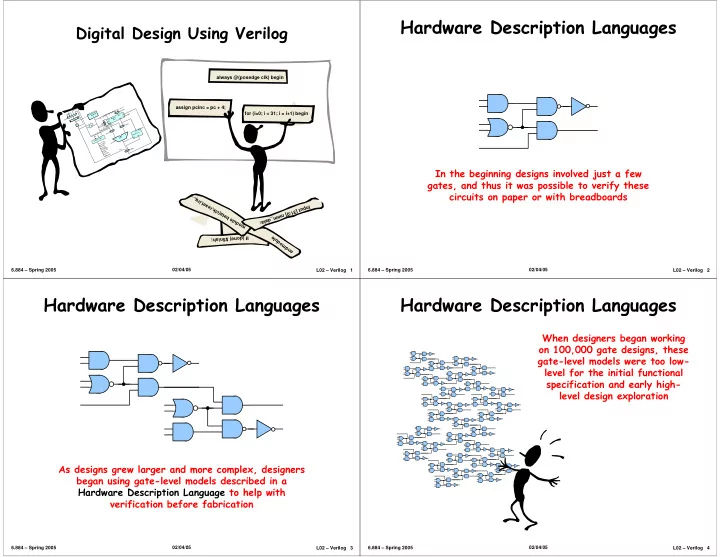
Hardware Description Languages
In the beginning designs involved just a few gates, and thus it was possible to verify these circuits on paper or with breadboards
L02 – Verilog 3 6.884 – Spring 2005 02/04/05
Hardware Description Languages
As designs grew larger and more complex, designers began using gate-level models described in a Hardware Description Language to help with verification before fabrication
L02 – Verilog 4 6.884 – Spring 2005 02/04/05
Hardware Description Languages
When designers began working
- n 100,000 gate designs, these
gate-level models were too low- level for the initial functional specification and early high- level design exploration