Lecture 3 Hardware and Software 3. Hardware and Softw are 4. - - PDF document

lecture 3
SMART_READER_LITE
LIVE PREVIEW

Lecture 3 Hardware and Software 3. Hardware and Softw are 4. - - PDF document

1. Introduction 2. Binary Representation Lecture 3 Hardware and Software 3. Hardware and Softw are 4. High Level Languages 5. Standard input and output Hardware has been defined as 6. Operators, expression and statem ents the


slide-1
SLIDE 1

1

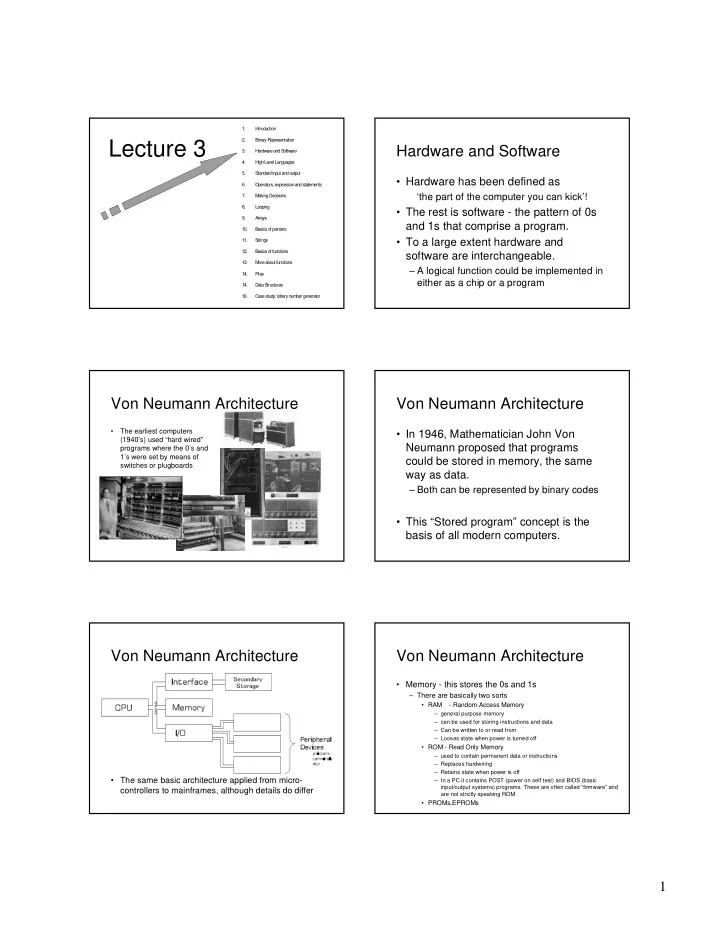
1. Introduction 2. Binary Representation 3. Hardware and Softw are 4. High Level Languages 5. Standard input and output 6. Operators, expression and statem ents 7. M aking Decisions 8. Looping 9. Arrays 10. Basics of pointers 11. Strings 12. Basics of functions 13. M

  • re about functions

14. Files 14. Data Struc tures 16. Cas e study: lottery num ber generator

Lecture 3

Hardware and Software

  • Hardware has been defined as

‘the part of the computer you can kick’!

  • The rest is software - the pattern of 0s

and 1s that comprise a program.

  • To a large extent hardware and

software are interchangeable.

– A logical function could be implemented in either as a chip or a program

Von Neumann Architecture

  • The earliest computers

(1940’s) used “hard wired” programs where the 0’s and 1’s were set by means of switches or plugboards

Von Neumann Architecture

  • In 1946, Mathematician John Von

Neumann proposed that programs could be stored in memory, the same way as data.

– Both can be represented by binary codes

  • This “Stored program” concept is the

basis of all modern computers.

Von Neumann Architecture

  • The same basic architecture applied from micro-

controllers to mainframes, although details do differ CPU Interface Memory I/O

Secondary Storage

Peripheral Devices

printers terminals etc

D A T A B U S

Von Neumann Architecture

  • Memory - this stores the 0s and 1s

– There are basically two sorts

  • RAM - Random Access Memory

– general purpose memory – can be used for storing instructions and data – Can be written to or read from – Looses state when power is turned off

  • ROM - Read Only Memory

– used to contain permanent data or instructions – Replaces hardwiring – Retains state when power is off – In a PC it contains POST (power on self test) and BIOS (basic input/output systems) programs. These are often called “firmware” and are not strictly speaking ROM

  • PROMs,EPROMs
slide-2
SLIDE 2

2

Von Neumann Architecture

  • Secondary Storage

– provides a further area for storing information – Can take many physical forms but most commonly magnetic disk storage – Can also have read only secondary storage eg CD-ROM – Typically

  • slower than main memory
  • larger storage than main memory
  • lower price per MB of memory

Von Neumann Architecture

  • CPU - Central Processing Unit

– The power behind the computer, contains

  • data registers (internal memory) for holding

data

  • address registers for holding memory

addresses

  • ALU - Arithmetic Logic Unit
  • Shift registers
  • Cache memory

Von Neumann Architecture

  • Buses

– a bus is simply a set of wires which act as a data highway for moving binary information around the computer

  • address bus
  • data bus
  • control bus

– 1 wire transmits one bit

Von Neumann Architecture

  • I/O - Input/Output

– forms the interface between the computer and external peripheral devices

  • Peripheral Devices

– Typically keyboard, display, printer, scanner, network adapter etc

Memory Map

  • Memory is organised into bytes (or words), each of

which must have its own unique address, so it can be identified

  • Suppose we have a 24-bit address bus, then there are

224=16,777,216 addresses which constitute our address space

  • The lowest is 000000hex and the highest FFFFFFhex

Memory Map - Addresses

8 bits

00 00 00 00 FF FF 8M RAM 02 00 00 7F FF FF 80 00 00 FF FF FF 01 FF FF NOT USED 64K I/O 64K ROM Boot loader etc. “low memory” Memory Mapped I/O Could be filled later General Purpose Memory “high memory”

slide-3
SLIDE 3

3

Memory Access - read/Write cycles

  • To read data from memory into the CPU

– The CPU puts the relevant address onto the address bus – The appropriate memory cell recognises its own address (actually performed by a circuit called an address decoder) – The CPU waits for this to happen then activates the read line – The memory cell connects its output to the databus – The CPU waits for this to happen then copies the data from the bus to an internal register – The CPU deactivates the read line, the memory cell is disconnected from the databus – The CPU removes the address from the address bus

  • NB all operations take a non-zero amount of time which

must be allowed for e.g. a memory read may take 100ns

Memory access

  • Write access is similar but the write line is activated

instead of the read line and hence the data is transferred from the CPU to the memory cell

  • It is important to be clear about the difference

between addresses and data. Both are binary codes

  • The address identifies a particular memory location
  • The data is the contents of that location

NB Here data includes instructions address 9A BC 2D Dr R Bowden