
SLIDE 1
Backend Tools
Place and Route for Faraday 130nm
Joachim Rodrigues
Lund University / Oskar Andersson / IC project 1/ Place and Route / 27 Jan 2015
Import Design
- This step will take a while. Be patient and pick exactly the files
specified in the guide.
- It is possible to save/load settings using the Save button.
Do this to avoid browsing for all files multiple times. This applies both to Design Import and Create Analysis Configuration.
- It is important that all files are included and in the correct order.
Look for possible errors in the command prompt.
- If you need to re-import your design the tool needs to be restarted.
2 Lund University / Oskar Andersson / IC project 1/ Place and Route / 27 Jan 2015
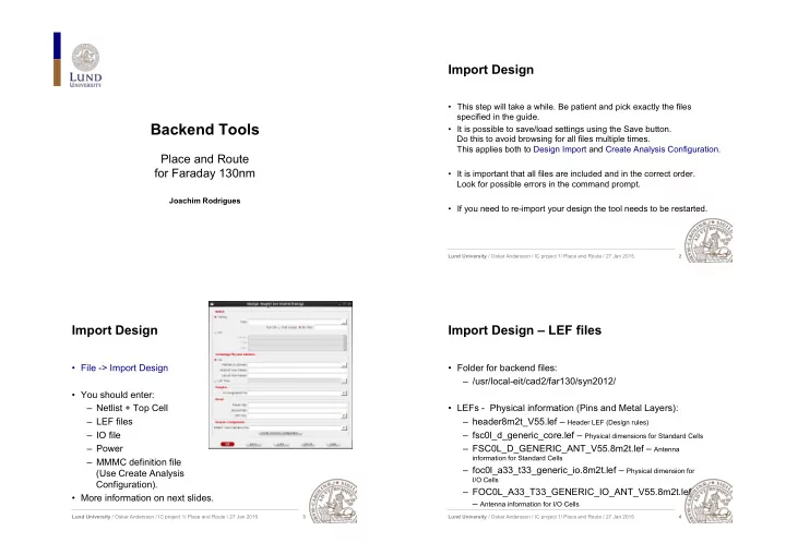
Import Design
- File -> Import Design
- You should enter:
– Netlist + Top Cell – LEF files – IO file – Power – MMMC definition file (Use Create Analysis Configuration).
- More information on next slides.
3 Lund University / Oskar Andersson / IC project 1/ Place and Route / 27 Jan 2015
Import Design – LEF files
- Folder for backend files:
– /usr/local-eit/cad2/far130/syn2012/
- LEFs - Physical information (Pins and Metal Layers):
– header8m2t_V55.lef – Header LEF (Design rules) – fsc0l_d_generic_core.lef – Physical dimensions for Standard Cells – FSC0L_D_GENERIC_ANT_V55.8m2t.lef – Antenna
information for Standard Cells
– foc0l_a33_t33_generic_io.8m2t.lef – Physical dimension for
I/O Cells
– FOC0L_A33_T33_GENERIC_IO_ANT_V55.8m2t.lef – Antenna information for I/O Cells
4