
SLIDE 1
ETI210 – IC Project and Verification
IC Project 2008 Introduction
Examiners: Prof. Henrik Sjöland (Analog+ Mixed)
- Dr. Joachim Rodrigues (Digital + Computer)
IC Project 2010 Introduction
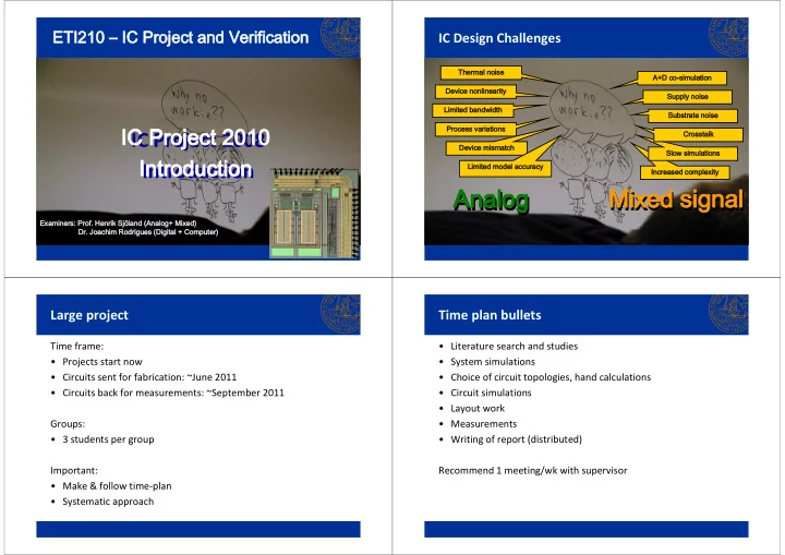
IC Design Challenges
Limited bandwidth Thermal noise Process variations Device nonlinearity Device mismatch Limited model accuracy Increased complexity Slow simulations Crosstalk Substrate noise A+D co-simulation
Analog Analog Mixed signal Mixed signal
Supply noise
Large project
Time frame:
- Projects start now
- Circuits sent for fabrication: ~June 2011
- Circuits back for measurements: ~September 2011
Groups:
- 3 students per group
Important:
- Make & follow time‐plan
- Systematic approach
Time plan bullets
- Literature search and studies
- System simulations
- Choice of circuit topologies, hand calculations
- Circuit simulations
- Layout work
- Measurements
- Writing of report (distributed)
Recommend 1 meeting/wk with supervisor