
SLIDE 1
Systems Design and Programming Basic I/O IV CMPE 310 1 (April 17, 2002)
UMBC
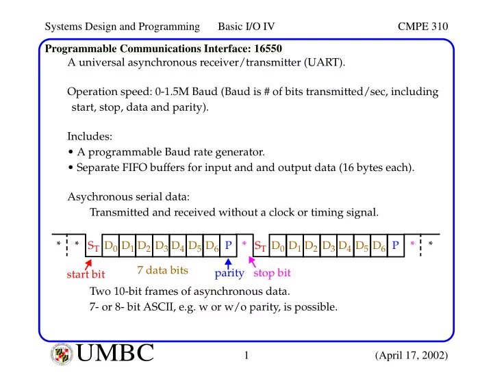
U M B C U N I V E R S I T Y O F M A R Y L A N D B A L T I M O R E C O U N T Y 1 9 6 6Programmable Communications Interface: 16550 A universal asynchronous receiver/transmitter (UART). Operation speed: 0-1.5M Baud (Baud is # of bits transmitted/sec, including start, stop, data and parity). Includes:
- A programmable Baud rate generator.
- Separate FIFO buffers for input and and output data (16 bytes each).
Asychronous serial data: Transmitted and received without a clock or timing signal. Two 10-bit frames of asynchronous data. 7- or 8- bit ASCII, e.g. w or w/o parity, is possible. D0 ST * * D1 D2 D3 D4 D5 D6 P * D0 ST D1 D2 D3 D4 D5 D6 P * * start bit 7 data bits parity stop bit