
SLIDE 1
Advanced VLSI Design Combination Logic Design I CMPE 640 1 (11/15/04)
UMBC
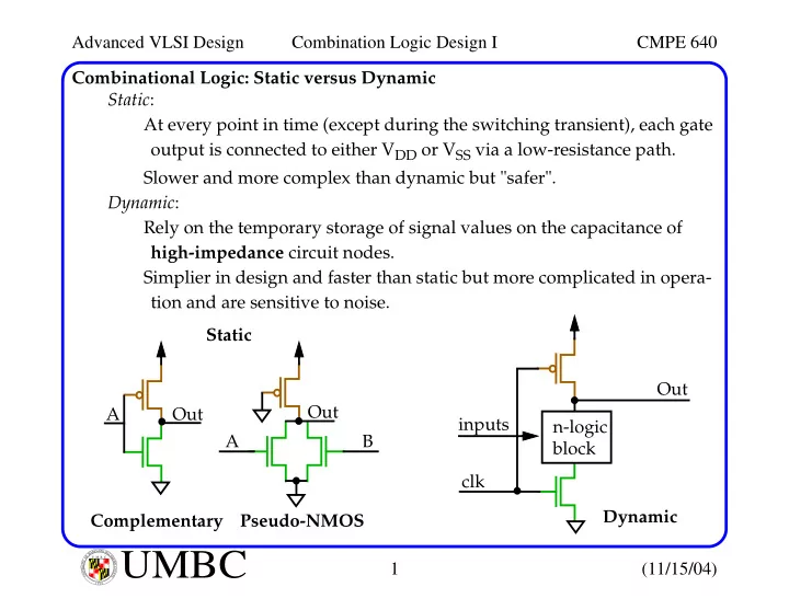
U M B C U N I V E R S I T Y O F M A R Y L A N D B A L T I M O R E C O U N T Y 1 9 6 6Combinational Logic: Static versus Dynamic Static: At every point in time (except during the switching transient), each gate
- utput is connected to either VDD or VSS via a low-resistance path.
Slower and more complex than dynamic but "safer". Dynamic: Rely on the temporary storage of signal values on the capacitance of high-impedance circuit nodes. Simplier in design and faster than static but more complicated in opera- tion and are sensitive to noise. A Out Out A Static Out n-logic block clk inputs B Dynamic Pseudo-NMOS Complementary