the need for more efficient electronics
play

The Need For More Efficient Electronics The Internet will soon have - PowerPoint PPT Presentation

The Need For More Efficient Electronics The Internet will soon have a carbon footprint equivalent to a large industrialized country -The Gaurdian- https://www.theguardian.com/environment/2010/aug/12/carbon-footprint-internet Googles Big


  1. The Need For More Efficient Electronics 
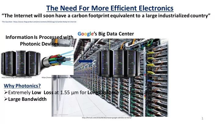
“The Internet will soon have a carbon footprint equivalent to a large industrialized country” -The Gaurdian- https://www.theguardian.com/environment/2010/aug/12/carbon-footprint-internet Google’s Big Data Center Information Is Processed with Photonic Devices http://www.pngmart.com/image/58330 https://www.merrymesh.com/fiber-optic-cable.html Why Photonics? Ø Extremely Low Loss at 1.55 μm for Long Distance communications Ø Large Bandwidth http://fortune.com/2016/09/30/amazon-google-add-data-centers / 1

  2. Waveguide Fundamentals n cladding 2D Waveguide Laser n1 n core n cladding n core > n cladding => undergoes total internal reflection and propagates through waveguide Reflected light forms standing Energy Distribution wave patterns called modes Amplitude 1 st Order Mode 2 Fundamental Mode

  3. Better Efficiency Solutions 1)Reduction of Modal Size Mismatch Optical Fiber Waveguide 3

  4. Fiber Vs Semiconductor Waveguide Mode Size 0 1.0 Fiber Waveguide Field Strength 10 μm 0.5 μm 4

  5. Better Efficiency Solutions 2) Reduce effective index to minimize power reflection 𝒐 𝒃𝒋𝒔 = 1 Optical Fiber Waveguide 𝒐 𝑫𝒎𝒃𝒆𝒆𝒋𝒐𝒉 𝒐 𝑫𝒑𝒔𝒇 𝒐 𝒇𝒈𝒈 > 𝟐 𝒐 𝑫𝒎𝒃𝒆𝒆𝒋𝒐𝒉 𝒐 𝒇𝒈𝒈 depends upon: 𝟑 𝒐 𝒇𝒈𝒈 %𝒐 𝒃𝒋𝒔 𝚫 = Ø 𝒐 𝑫𝒑𝒔𝒇 & 𝒐 𝑫𝒎𝒃𝒆𝒆𝒋𝒐𝒉 𝒐 𝑫𝒎𝒃𝒆𝒆𝒋𝒐𝒉 < 𝒐 𝒇𝒈𝒈 < 𝒐 𝑫𝒑𝒔𝒇 𝒐 𝒇𝒈𝒈 )𝒐 𝒃𝒋𝒔 Ø Waveguide geometry 5

  6. Waveguide Design using Rsoft BeamPROP GaAs Waveguide a-Si Waveguide 6

  7. GaAs Waveguide Cross-Sectional View Width Mode Profile 0.05 μm 0.65 μm AlGaAs (n = 2.939) GaAs (n = 3.377) 0.42 μm 1.2 μm AlGaAs (n = 2.939) Si Substrate 7

  8. GaAs Waveguide Taper designed to reduce effective index 𝒐 𝒇𝒈𝒈 𝛃 w 8

  9. a-Si Waveguide w 𝒐 𝒇𝒈𝒈 𝛃 w a-Si Waveguide Cover Material Options BCB Upper Cladding Si 3 N 4 Upper Cladding (n=1.535) (n=1.91) a-Si a-Si BCB Lower Cladding BCB Lower Cladding (n = 1.535) (n = 1.535) Si Substrate Si Substrate 9 v

  10. Concept 1.55 μm a-Si Waveguide Fiber laser Mode profile gradually varies along taper 10

  11. a-Si with BCB Cladding Index Matching Results BCB Upper Cladding (n=1.535) t = .1μm w = .25μm w = .7μm N eff = 2.076 a-Si GaAs a-Si BCB Lower Cladding (n = 1.535) Si Substrate 11

  12. a-Si with SiN 4 Cladding Index Matching Results Si 3 N 4 Cladding (n=1.91) t = .1μm w = 1.2μm a-Si w = .29μm N eff = 2.287 BCB Substrate N = 1.535 a-Si GaAs Si Substrate 12

  13. Power Efficiency GaAs a-Si Removing top two layers of structure

  14. Conclusions and Future Work In general, III-V waveguides have tightly confined modes which are undesired. By introducing the tapered design, I have demonstrated a low loss passive coupling interface with a larger mode profile. I have also simulated the coupling loss into the Si waveguide – approximately 3.9dB per coupling interface. By reducing the Si waveguide width further, we can reduce this loss. 14

  15. Acknowledgements Wendy Ibsen (Program Coordinator) Prashanth Bhasker (Graduate Mentor) Jhonattan Ramirez (Post Doctoral Researcher) Dr. Nadir Dagli (Principal Investigator) 15

Download Presentation
Download Policy: The content available on the website is offered to you 'AS IS' for your personal information and use only. It cannot be commercialized, licensed, or distributed on other websites without prior consent from the author. To download a presentation, simply click this link. If you encounter any difficulties during the download process, it's possible that the publisher has removed the file from their server.

Recommend


More recommend