SLIDE 1
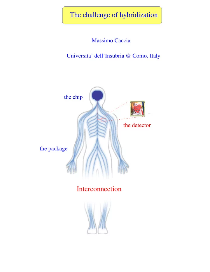
Massimo Caccia Universita’ dell’Insubria @ Como, Italy the package
The challenge of hybridization
the detector the chip
Interconnection
SLIDE 2
running for 8 months/year without hw interventions since 1997
strips pixels
completed and installed in 1996 a case study: the DELPHI pixel detector
SLIDE 3 a "relaxed" detector:
material budget: 300 + 300 micron (Si) + 300 micron (Kapton)
"mass" production: 152 modules, for a total of 1.2 M pixels
pixel cell size: 330 micron x 330 micron temperature: - operating at room T
- 10 C gradient along the 7 cm long module acceptable
radiation hardness: << Krad/year mechanical tolerances readout speed: 5 MHz precision mounting/alignment nevertheless......
SLIDE 4 J.M. Heuser DELPHI Pixel Detector – Running Experience & System Features
- Int. Conf. on Advanced Technology & Particle Physics, Como, Italy, 1998
23 (8.5%) 14 (5.2%) 10 (3.7%) 7 (2.6%) 4 (1.5%) 34 (12.5%) 35 (12.9%) 52 (19.2%) 10 20 30 40 50 60 decoding errors rate high dark current noisy short circuits broken (ceramics) missing signals of a chip kapton problems
Pixel detector production yield
final test: breakdown of errors
"learning curve": ~30% --> ~60% total production efficiency: 36% module assembly most critical
SLIDE 5
the next generation: pixel detectors for the future hadron colliders
a sketch of the ATLAS pixel detector ~2 m real "mass" production: ~ 2200 modules (16 chips each), sensor + VLSI : substrate for power bus, : mechanical support ~140 M pixels in total minimal pixel pitch: 50 micron data & control lines material budget is an issue! ratio of the different contributions (in X_0)
1 : 0.4 : 1.5
SLIDE 6
very limited clearance : O(1 mm) assembled at room temperature, operated at -5 to -10 C, with possible gradients at the 2-3 C level nevertheless, a global yield at the 70% level is the goal to be achieved to 1.18 mm radiation hard: have the detector completed clocked at 40 MHz
SLIDE 7 topside metallurgy
&
detector Front end chip
Due to the bond density (~ 5000-10000 / cm ) and the pitch
2
(~ 50 m) µ the only meaningful interconnection technique is BUMP BONDING
BUMP Under Bump Metal
final chip metal via
under bump metallization bonding mechanism => - temperature
The choice of the bump metal determines the processing characteristics: aspect ratio => - pitch
- single/double sided process
mechanical properties => - tensile/shear strength
- "reworkability"
- alignment precision
Front-end chip to sensor connection
SLIDE 8 reflow occurs at different temperatures, depending on the solder mix and ranging between 230C (63SnPb) to 360 C (5SnPb).
Solder bumps
the limits of wire bonding Solder bump bonding has been introduced ~ 30 year ago by IBM (C4 processing = Controlled Collapse Chip Connection) to overcome Reflow may occur in presence of a suitable flux or in a fluxless process, UBM = Under Metal Bump: possibly in a batch of organic compound
- adhesion layer (active metal) on top of the final metal pad ( Cr or TiW)
- barrier metal to prevent the solder dissolving the active metal (Cr-Cu or Cu)
- Solder wettable metal (Cu)
- Oxide prevention (Au)
SLIDE 9
- apply a resin-based flux, for fixing the chip
solder bump
- move the assembly to a furnace for reflowing
(neutral atmosphere)
- align the chip to the substrate and place it (~0 pressure)
Self-aligning/planarizing properties of the solder bumps: wettable substrate pad
SLIDE 10 remarks strong points:
uniformity & self-alignment => low % of missed contacts thermal fatigue of bumps should not be neglected
- ptimal height/pitch ratio (~20 micron/50 micron)
=> bump grown on one side only excellent electrical properties ( contact resistance ~ mOhm) result in poor adhesion "high" Temperature: it may harm rad-hard chips complex UBM: a not perfect control of the metallurgy may "reflow" chemistry: "leftover" might affect wire bondability; Hydrogen entrapment may result in voiding pitch for detector applications at the edge of the industrial standards (~150 micron, 70 micron footprint)
critical points:
SLIDE 11 after D.S. Patterson et al, Flip Chip Technologies (http://www.flipchip.com): (in number of cycles) experimental conditions:
- bump diameter: 100 micron
- thermal cycle range: -50 C to 150 C
- substrate: Alumina, 0.5" x 0.5"
SLIDE 12
before after reflow WA97/RD19: 0.5 M pixels, 50 x 500 micron size,
fault rate ~ 10 ppm
bump bonded by GEC-Marconi DELPHI: 1.2 M pixels, 330 x 330 micron size, bump bonded by IBM ATLAS: test structures & prototypes bonded by IZM, Berlin; 50 x 400 micron size achievements
SLIDE 13
- perating at liquid N temperature.
Indium bumping technology refined for IR sensors (Focal Plane Arrays),
Indium bumps
patterining of photoresist evaporation of barrieri metal layer lift off / patterining of
=> bump grown on both sides
thick photoresist evaporation of Indium lift off Al pad photoresist passivation UBM 5-10 micron bump startup
after electrical breakdown, the contact resistance is O(1 Ohm) because of In oxidation, "reflowing" In bumps is far from being "trivial" chemical etching of the holes and evaporation have to be under good control and bumps have a small height/pitch ratio (5 micron/50 micron) in order to avoid In to be smashed against the photoresist walls,
SLIDE 14 remarks critical points: high yield attachment requires excellent planarity and bump uniformity pitch for detector applications well within industrial standards strong points: simple UBM: a Cr adhesion layer will do it bonding by solid state diffusion => it requires little pressure "small" bumps require a "double sided process"
(~10 N/bump) at temperatures ranging between 20-100C (~30 micron pitch) Indium plastic properties should help against thermal fatigue but intensive tests should be considered
SLIDE 15
achievements ALENIA (Italy), SOFRADIR (FRANCE) on ATLAS level have been achieved with a fair/good control of systematics: pixel modules PSI (Switzerland) on CMS modules have gone far beyond a feasibility study; fault rates at the 10 ppm
SLIDE 16 conclusions on the front-end to sensor interconnection both In and Solder bumps have proven to have an acceptable are not an alternative by now single bump failure the choice is defined by "side effects", process control and repeatibility reworking is also an issue
- ther interconnection techniques (ACF, stencil printing, stud bonding)
SLIDE 17 stripping @ 100 C T B IN BOTH CASES In IS LEFT ON BOTH SIDES
These is how the bumps appear after being stripped at 100 C:
T B
x
T is flipped
a quite isotropical detachment was
assemblies at Milano/Insubria
SLIDE 18 reworking
test structures in terms of:
A dedicated "chip-stripping" machine has been designed and it’s being built
The possibility of re-working has been assessed by the analysis of tensile strength of the structure: decreased by 20% single bump electrical fault rate: 0/50 contacts missing on 3 structures characterization of a re-worked real detector: ~ 10% missing pixels
- n a "single chip" assembly
SLIDE 19
Three approaches:
the detector BACKPLANE
"flex" hybrid:
front-end chips POwer/DC flex cable Optical fiber bias flex cable SMD wire bonds Optopackage temperature sensors Clock & control chip
FLEX on
Power lines and signal bus
SLIDE 20 ~ 2cm ~ 7 cm
ATLAS specifications: - 2 metal layers
* kapton substrate, metal traces on both faces (25 micron thick) * Copper traces: 7 m thick, 75 m minimal distance,
critical issues:
75 m minimal space * top/bottom cover layer: 12.5 m thick µ µ µ µ
- wire bonds
- stress induced on the bumps:
support chips detector flex
material CTE (* 10 C )
CC (support) -1 (in plane) 6 (transverse) Silicon 2.5 flex ~ 45
SLIDE 21
SLIDE 22
SLIDE 23 "wireless" application: an MCM-D approach MCM-D = Multi Chip Module with Deposited Dielectric:
chips
- thin film technology
- interconnections formed depositing dielectric material
r
- n the junction side of the sensor:
ε (BCB = benzocyclobutene, = 2.7)and conductors
support
detector MCM-D
SLIDE 24 a study by the Wuppertal team + IZM, IMEC for the ATLAS pixels: main characteristics:
- 4 copper layers, for the signal & power bus at the chip edge
(thickness: 4-10 micron/layer)
- no wire bonding: Front end I/O also connected by bump bonding
- traces: 20 micron width, 2 micron thick, 30 micron spacing
- interconnection of the pixels to the fron-end cell through
a "staircase":
SLIDE 25 strong points:
- wireless, robust, "monolithic"
- "easy" to implement a monting scheme limiting the
stress induced by CTE mismatches on the bumps critical issues:
- wireless, robust, "monolithic"
=> the fault rate on the bump bonds HAS to be at the 10 ppm as the chips I/O are also bump bonded the MCM-D process can be re-done on the same substrate => the staircase feed through connections from the pixel cells to the mating front end cell has to be quite reliable...
- 4 vias / cell
- ~ 250 000 vias/ module
=> the interconnection is necessarily tested after it has been grown on the detector substrate, so it has to be made sure
SLIDE 26 The "integrated" technologies are certainly appealing but processing The "flex" hybrid technology is "under control"; special care should
- ptimization is still inder way
be paid to mounting issues (stress on bumps and wire bonds) conclusions on power & signal bus
SLIDE 27 10 cm
following the trend in the consumer electronics for portable devices: tt @ 550 GeV TESLA will be more compact.... linear collider
- (much) less material (< 0.3 % X_o / layer)
- higher resolution (~ 5 micron)
ext generation of Pixel detectors will require: