
SLIDE 1
Cl i ck t o edi t Mast er t i t l e st yl e
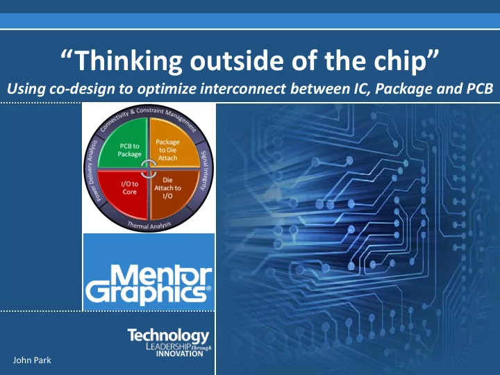
“Thinking outside of the chip”
Using co-design to optimize interconnect between IC, Package and PCB
John Park
Thinking outside of the chip Using co-design to optimize - - PowerPoint PPT Presentation
Cl i ck t o edi t Mast er t i t l e st yl e Thinking outside of the chip Using co-design to optimize interconnect between IC, Package and PCB John Park Current Over-the-wall design process Cl i ck t o edi t Mast er t i t l e st
John Park
IC Layout Package design PCB layout
Higher Cost
Custom package & Increased layers on PCB
Longer Development Cycles
Increased complexity for PCB and Package
IC Layout Package design PCB layout
Core Blocks RDL Routing Flip-chip bumps Package Pins (Balls) Die abstract PCB footprint (could include breakout)
I/O Buffers Off-Chip Passives
Implementation (Back-end)
Logic Design (Front-end)
RTL Entry Simulation Synthesis Simulation
Floor-planning Place & Route
Extraction Timing Verification Physical Verification
Verification & Analysis
IC place & route Package design Board design
PCB level footprint Placement Break-out routing Constraint assignment
Constraints, Connectivity, Physical placement
Package symbol Bump array generation Connectivity optimization Constraint assignment PCB level footprint Pin delays Accurate package model IO placement Connectivity assignment Constraint assignment RDL routing
What format is used for data exchange? Which design tool and team is responsible for what…
Stacked die Package on Package (PoP) 3D IC with TSV interconnect
Connectivity & Constraint capture Signal mapping between IC, Package and PCB
Physical based unraveling (optimizing) environment PCB to Package Optimization Package to Die Attach Optimization (Bond Finger or Bump) Die Attach to I/O Optimization I/O to Core Optimization
Physical Instances/ Abstracts
Swap Rules
Bus Standards User Defined
IC floorplan Package Pin-out PCB Placement
Before optimization After optimization
Courtesy of: