
SLIDE 1
1
Computer System Architecture Processor Part I
Chalermek Intanagonwiwat
Slides courtesy of John Hennessy and David Patterson
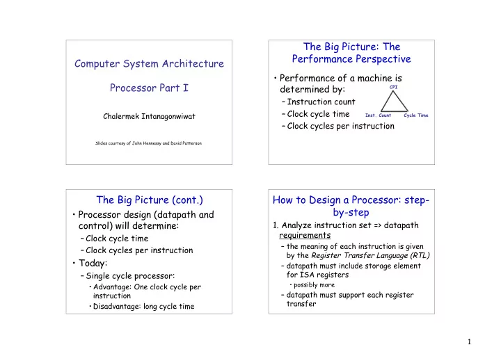
The Big Picture: The Performance Perspective
- Performance of a machine is
determined by:
– Instruction count – Clock cycle time – Clock cycles per instruction
CPI
- Inst. Count
Cycle Time
The Big Picture (cont.)
- Processor design (datapath and
control) will determine:
– Clock cycle time – Clock cycles per instruction
- Today:
– Single cycle processor:
- Advantage: One clock cycle per
instruction
- Disadvantage: long cycle time
How to Design a Processor: step- by-step
- 1. Analyze instruction set => datapath
requirements
– the meaning of each instruction is given by the Register Transfer Language (RTL) – datapath must include storage element for ISA registers
- possibly more