
SLIDE 1
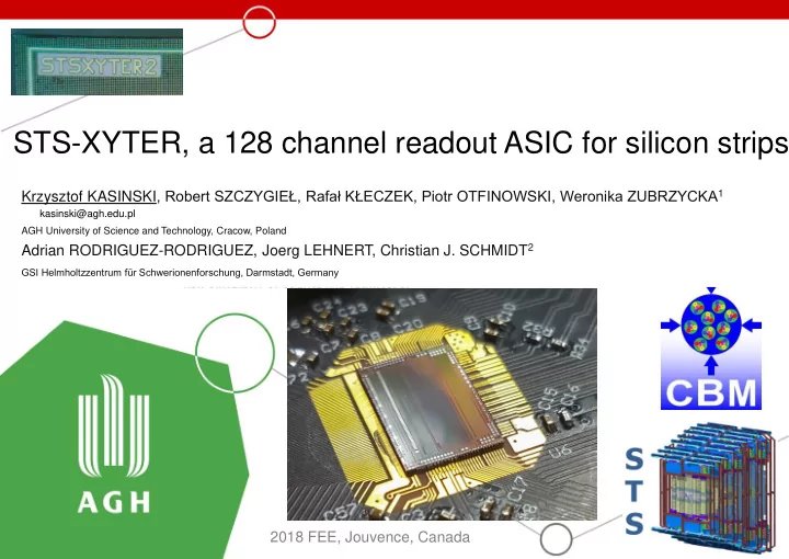
STS-XYTER, a 128 channel readout ASIC for silicon strips
2018 FEE, Jouvence, Canada Krzysztof KASINSKI, Robert SZCZYGIEŁ, Rafał KŁECZEK, Piotr OTFINOWSKI, Weronika ZUBRZYCKA1
AGH University of Science and Technology, Cracow, Poland
Adrian RODRIGUEZ-RODRIGUEZ, Joerg LEHNERT, Christian J. SCHMIDT2
GSI Helmholtzzentrum für Schwerionenforschung, Darmstadt, Germany kasinski@agh.edu.pl