
SLIDE 1
EEL7312 – INE5442 Digital Integrated Circuits 1
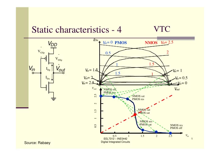
Source: Rabaey
Static characteristics - 4
Vin Vout V
DD
- VGSp
+
- VDSp
+
IDp IDn
IDn V
- ut
V
in= 2.5
2 1.5 V
in= 0
0.5 1 NMOS V
in= 0
V
in= 0.5
V
in= 1
V
in= 1.5
V
in= 2
V
in= 2.5
1 1.5 PMOS
VTC
Vout 0.5 1 1.5 2 2.5 NMOS res PMOS off NMOS sat PMOS sat NMOS off PMOS res NMOS sat PMOS res NMOS res PMOS sat
in
0.5 1 1.5 2 2.5 V