Page 1 Ingrid Verbauwhede, KU Leuven COSIC, ALBENA, July 2013 - - PowerPoint PPT Presentation

page 1
SMART_READER_LITE
LIVE PREVIEW

Page 1 Ingrid Verbauwhede, KU Leuven COSIC, ALBENA, July 2013 - - PowerPoint PPT Presentation

Goal Digital Circuits: Fundamental understanding of CMOS circuits why they leak, how to counter Ingrid Verbauwhede So as to build models Ingrid.verbauwhede-at-esat.kuleuven.be And understand short comings of models KU Leuven, COSIC


slide-1
SLIDE 1

Page 1

Ingrid Verbauwhede, KU Leuven COSIC, ALBENA, July 2013

KU Leuven - COSIC Digital CMOS - 1 Albena, July 2013

Digital Circuits: why they leak, how to counter

Ingrid Verbauwhede Ingrid.verbauwhede-at-esat.kuleuven.be KU Leuven, COSIC Acknowledgements: Current and former Ph.D. students

KU Leuven - COSIC Digital CMOS - 2 Albena, July 2013

Goal

  • Fundamental understanding of CMOS circuits
  • So as to build models
  • And understand short comings of models

KU Leuven - COSIC Digital CMOS - 3 Albena, July 2013

Design for security: Countermeasures at every abstraction layer

Cipher Design, Biometrics

D Q Vcc

CPU Crypto MEM JCA Java JVM

CLK

Secure channel

SIM D Q Vcc

CPU MEM JCA Java KVM

CLK

OS: Operating system Crypto Algorithm/Protocol: Embedded fingerprint matching, crypto, entity authentication Architecture: Co-design, HW/SW, SOC Circuit: Circuit techniques to combat side channel analysis attacks Micro-Architecture: co-processor design

SIM SIM SIM

Weakest link decides security of the chain

Application: e-commerce, smart energy

KU Leuven - COSIC Digital CMOS - 4 Albena, July 2013
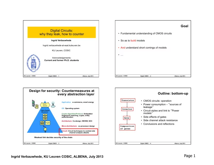
Outline: bottom-up

  • CMOS circuits: operation
  • Power consumption – “sources of

leakage”

  • Circuit styles and link to “Power

models”

  • Side effects of gates
  • Side channel attack resistance
  • Conclusions and reflections

Transistor Invertor Gate Composition

  • f gates
slide-2
SLIDE 2

Page 2

Ingrid Verbauwhede, KU Leuven COSIC, ALBENA, July 2013

KU Leuven - COSIC Digital CMOS - 5 Albena, July 2013

Outline

  • CMOS circuits: operation
  • Power consumption – “sources of

leakage”

– Current – Dynamic power – Static power

Transistor Invertor

KU Leuven - COSIC Digital CMOS - 6 Albena, July 2013

CMOS invertor

power and energy fundamentals

KU Leuven - COSIC Digital CMOS - 7 Albena, July 2013

The CMOS Inverter: A First Glance

V

in

V

  • ut

C

L

V

DD

Slide courtesy: J. Rabaey KU Leuven - COSIC Digital CMOS - 8 Albena, July 2013

The image cannot be

  • displayed. Your

computer may not have enough memory to open the image, or the image may have been corrupted. Restart your computer, and then

  • pen the file again. If

the red x still appears, you may have to delete the image and then insert it again.

CMOS Inverter

Polysilicon In Out V DD GND PMOS 2λ Metal 1 NMOS

Out In VDD PMOS NMOS

Contacts N Well

Slide courtesy: J. Rabaey

slide-3
SLIDE 3

Page 3

Ingrid Verbauwhede, KU Leuven COSIC, ALBENA, July 2013

KU Leuven - COSIC Digital CMOS - 9 Albena, July 2013

Two Inverters

Connect in Metal

Share power and ground Abut cells

VDD

Slide courtesy: J. Rabaey KU Leuven - COSIC Digital CMOS - 10 Albena, July 2013

CMOS Inverter: First-Order DC Analysis VOL = 0 VOH = VDD VM = f(Rn, Rp)

V

DD

V

DD

V

in 5 V DD

V

in 5 0

V

  • ut

V

  • ut

R

n

R

p

Slide courtesy: J. Rabaey

Why we like CMOS!!

= STATIC behavior

KU Leuven - COSIC Digital CMOS - 11 Albena, July 2013

CMOS Inverter: Transient Response

t

pHL

= f(R

  • n

.C

L

) = 0.69 R

  • n

C

L V

  • ut

V

  • ut

R

n

R

p

V

DD

V

DD

V

in 5 V DD

V

in 5 0

(a) Low-to-high (b) High-to-low C

L

C

L

Slide courtesy: J. Rabaey

= DYNAMIC behavior

KU Leuven - COSIC Digital CMOS - 12 Albena, July 2013

Where Does Power Go in CMOS?

  • Dynamic Power Consumption
  • Charging and discharging capacitors
  • Short Circuit Currents
  • Short circuit path between supply rails

during switching

  • No longer an issue in deep submicron
  • Leakage
  • Leaking diodes and transistors
slide-4
SLIDE 4

Page 4

Ingrid Verbauwhede, KU Leuven COSIC, ALBENA, July 2013

KU Leuven - COSIC Digital CMOS - 13 Albena, July 2013

Dynamic Power Dissipation

Energy/transition = C

L

* V

dd 2

Power = Energy/transition * f = C

L

* V

dd 2

* f Need to reduce C

L

, V

dd

, and f to reduce power.

Vin Vout C

L

T h e i m

Vdd

Not a function of transistor sizes!

KU Leuven - COSIC Digital CMOS - 14 Albena, July 2013

Vout

Vdd

Sub-Threshold Current Drain Junction Leakage

Sub-threshold current one of most compelling issues in low-energy circuit design!

  • Strong function of temperature
  • New source of side-channel leakage = State!

Leakage current

KU Leuven - COSIC Digital CMOS - 15 Albena, July 2013

Outline

  • CMOS circuits: operation
  • Power consumption – “sources of leakage”
  • Circuit styles and link to “Power models”

– Static CMOS – Dynamic, pre-charged CMOS – Differential CMOS – Dynamic – differential CMOS – Link to Hamming Weight – Hamming Distance

  • Side effects of gates
  • Side channel attack resistance
  • Conclusions and reflections

Gate

KU Leuven - COSIC Digital CMOS - 16 Albena, July 2013

Static CMOS

Basics and construction rules

slide-5
SLIDE 5

Page 5

Ingrid Verbauwhede, KU Leuven COSIC, ALBENA, July 2013

KU Leuven - COSIC Digital CMOS - 17 Albena, July 2013

Static Complementary CMOS

VDD F(In1,In2,…InN) In1 In2 InN In1 In2 InN PUN PDN PMOS only NMOS only PUN and PDN are dual logic networks

… …

KU Leuven - COSIC Digital CMOS - 18 Albena, July 2013

NMOS Transistors in Series/Parallel Connection

Transistors can be thought as a switch controlled by its gate signal NMOS switch closes when switch control input is high

X Y A B Y = X if A and B X Y A B Y = X if A OR B

NMOS Transistors pass a “strong” 0 but a “weak” 1

KU Leuven - COSIC Digital CMOS - 19 Albena, July 2013

PMOS Transistors in Series/Parallel Connection

X Y A B Y = X if A AND B = A + B X Y A B Y = X if A OR B = AB

PMOS Transistors pass a “strong” 1 but a “weak” 0

PMOS switch closes when switch control input is low

KU Leuven - COSIC Digital CMOS - 20 Albena, July 2013

Complementary CMOS Logic Style

slide-6
SLIDE 6

Page 6

Ingrid Verbauwhede, KU Leuven COSIC, ALBENA, July 2013

KU Leuven - COSIC Digital CMOS - 21 Albena, July 2013

Example Gate: NAND

KU Leuven - COSIC Digital CMOS - 22 Albena, July 2013

Example Gate: NOR

Quiz: preference for NAND or NOR?

KU Leuven - COSIC Digital CMOS - 23 Albena, July 2013

Complex CMOS Gate

OUT = D + A • (B + C) D A B C D A B C

KU Leuven - COSIC Digital CMOS - 24 Albena, July 2013

Static CMOS Properties: ROBUST

  • Full rail-to-rail swing; high noise margins
  • Logic levels not dependent upon the relative device sizes;

ratioless

  • Always a path to Vdd or Gnd in steady state; low output

impedance

  • Extremely high input resistance; nearly zero steady-state input

current

  • No direct path steady state between power and ground; no static

power dissipation

  • Propagation delay function of load capacitance and resistance of

transistors

  • Style of choice for standard cell based design!
slide-7
SLIDE 7

Page 7

Ingrid Verbauwhede, KU Leuven COSIC, ALBENA, July 2013

KU Leuven - COSIC Digital CMOS - 25 Albena, July 2013

Standard Cell Zoom In

layout

vdd vss

KU Leuven - COSIC Digital CMOS - 26 Albena, July 2013

Module Generation

For data-path operators: structure is in bit-slices Computer generated layout as function of wordlength Compact, predictable IP

Power Instruction, Clock Data

KU Leuven - COSIC Digital CMOS - 27 Albena, July 2013

Standard Cell and Module

Courtesy: J. Van Campenhout RUG

Datapath Standard Cell Random Logic Few levels of metal

KU Leuven - COSIC Digital CMOS - 28 Albena, July 2013

More levels of metal: top levels not shown

slide-8
SLIDE 8

Page 8

Ingrid Verbauwhede, KU Leuven COSIC, ALBENA, July 2013

KU Leuven - COSIC Digital CMOS - 29 Albena, July 2013

Dynamic CMOS

Basics and construction rules

KU Leuven - COSIC Digital CMOS - 30 Albena, July 2013

Dynamic CMOS

  • In static circuits at every point in time (except when

switching) the output is connected to either GND or VDD via a low resistance path.

– fan-in of n requires 2n (n N-type + n P-type) devices

  • Dynamic circuits rely on the temporary storage of signal

values on the capacitance of high impedance nodes.

– requires on n + 2 (n+1 N-type + 1 P-type) transistors

KU Leuven - COSIC Digital CMOS - 31 Albena, July 2013

Dynamic Gate

In1 In2 PDN In3

Me Mp

Clk Clk Out CL Out Clk Clk A B C

Mp Me

Two phase operation Precharge (Clk = 0) Evaluate (Clk = 1)

  • n
  • ff

1

  • ff
  • n

((AB)+C)

KU Leuven - COSIC Digital CMOS - 32 Albena, July 2013

Conditions on Output

  • Once the output of a dynamic gate is discharged, it cannot

be charged again until the next precharge operation.

  • Inputs to the gate can make at most one transition during

evaluation.

  • Output can be in the high impedance state during and after

evaluation (PDN off), state is stored on CL Thus by construction, dynamic gates cannot glitch!

slide-9
SLIDE 9

Page 9

Ingrid Verbauwhede, KU Leuven COSIC, ALBENA, July 2013

KU Leuven - COSIC Digital CMOS - 33 Albena, July 2013

Cascading Dynamic Gates

Clk Clk Out1 In

Mp Me Mp Me

Clk Clk Out2 V t Clk In Out1 Out2 ΔV VTn

Only 0 → 1 transitions allowed at inputs!

KU Leuven - COSIC Digital CMOS - 34 Albena, July 2013

Domino Logic

In1 In2 PDN In3

Me Mp

Clk Clk Out1 In4 PDN In5

Me Mp

Clk Clk Out2

Mkp

1 → 1 1 → 0 0 → 0 0 → 1

All inputs to dynamic gate are set to 0 at end of precharge phase. So only 0 to 1 possible during evaluation. Moreover, bottom clk transistor is not needed.

KU Leuven - COSIC Digital CMOS - 35 Albena, July 2013

Why Domino?

Clk Clk Ini PDN Inj Ini Inj PDN Ini PDN Inj Ini PDN Inj

Like falling dominos!

KU Leuven - COSIC Digital CMOS - 36 Albena, July 2013

Differential (Dual Rail) Domino

A B

Me Mp

Clk Clk Out = AB !A !B

Mkp

Clk Out = AB

Mkp Mp

Solves the problem of non-inverting logic Can build complex pull-down networks

1 0 1 0

  • n
  • ff
slide-10
SLIDE 10

Page 10

Ingrid Verbauwhede, KU Leuven COSIC, ALBENA, July 2013

KU Leuven - COSIC Digital CMOS - 37 Albena, July 2013

Circuits against side channel attacks

How they leak How to solve it

KU Leuven - COSIC Digital CMOS - 38 Albena, July 2013

Static CMOS leaks information

  • Consumes power when output makes a 0 to 1 transition
  • Relation between previous and new value is visible

0-1 transition IN OUT 0 0 0 1 discharge 1 0 charge 1 1

KU Leuven - COSIC Digital CMOS - 39 Albena, July 2013

Static CMOS leaks Hamming Distance

  • R := reference state

– Which bit pattern was previously present? E.g. A pre-charged value An opcode on the bus A previously stored value

  • Hamming Weight := number of bits set to '1’
  • Power model:

a,b are constant, linear model

b R k x SBox HW a

i

+ ⊗ " ⊗ × ) ) ( (

KU Leuven - COSIC Digital CMOS - 40 Albena, July 2013

Duplicate logic: leaks Hamming distance

  • Distance between old and new value leaks

1

  • transition

0-1 transition IN IN OUT OUT 0 0 1 1 0 1 1 0 discharge charge 1 0 0 1 charge discharge 1 1 0 0

slide-11
SLIDE 11

Page 11

Ingrid Verbauwhede, KU Leuven COSIC, ALBENA, July 2013

KU Leuven - COSIC Digital CMOS - 41 Albena, July 2013

Dynamic logic: leaks Hamming weight

  • Dynamic logic breaks input

sequence

  • No longer dependent on

previous value

in

  • ut

Pr(echarge) Ev(aluation) PDN IN OUTPre OUTEV Charge 0 0 1 1 0 1 1 discharge 1 0 1 1 1 1 1 discharge

KU Leuven - COSIC Digital CMOS - 42 Albena, July 2013

Pre-charged bus leaks Hamming weight

KU Leuven - COSIC Digital CMOS - 43 Albena, July 2013

Transition independent power consumption …

  • When logic values are measured by charging and

discharging capacitances, we need to use a fixed amount of energy for every transition

switch once every cycle switch a constant load capacitance § …doesn’t create any side channel information § No Hamming distance, No Hamming weight

KU Leuven - COSIC Digital CMOS - 44 Albena, July 2013

Dynamic and Differential logic …

  • is necessary but not sufficient

AND NAND A B B clk clk A (1,1) input (0,0) input

→ Balance differential output nodes → (Dis)charge all internal nodes

E.g. DCVSL is not sufficient

[Tiri,ESSCIRC02]

slide-12
SLIDE 12

Page 12

Ingrid Verbauwhede, KU Leuven COSIC, ALBENA, July 2013

KU Leuven - COSIC Digital CMOS - 45 Albena, July 2013

Sense Amplifier Based Logic charges each cycle a constant load

clk AND NAND clk A B A B clk VDD M1

  • Balanced input and
  • utput nodes
  • All internal nodes

connect to an output

KU Leuven - COSIC Digital CMOS - 46 Albena, July 2013

Sense Amplifier Based Logic

AND NAND

Ctot=19.32fF

AND NAND

Ctot=19.38fF

KU Leuven - COSIC Digital CMOS - 47 Albena, July 2013

Solution based on Standard cells

  • false output
  • with false inputs

B A Z A B A B Z Z A B A prch Z B Z

De-Morgan’s Law AND-ing with precharge signal 1 2

§ precharge 1:

  • utputs are 0

§ precharge 0 - evaluation: 1 output is 1

KU Leuven - COSIC Digital CMOS - 48 Albena, July 2013

Wave Dynamic Differential Logic

  • Restrict library to AND, OR gate

– input 0 ⇒ output 0 – no precharge operator AND gate OR gate prch precharge inputs clk Encryption Module register clk

eval. prch.

[Tiri,DATE2004]

slide-13
SLIDE 13

Page 13

Ingrid Verbauwhede, KU Leuven COSIC, ALBENA, July 2013

KU Leuven - COSIC Digital CMOS - 49 Albena, July 2013

  • All functions of and2, or2 operator
  • In addition: inverted input, output signals
  • XOR2X4: OAI221X2:
  • Our WDDL library: 128 cells

WDDL library

A

A B B Y Y

AOI22X1 OAI22X1 INVX4 INVX4

C0

OAI221X1 AOI221X1

A0 A1 B0 B1 Y Y

INVX2 INVX2

A0 A1 B0 B1 C0 KU Leuven - COSIC Digital CMOS - 50 Albena, July 2013

WDDL Example

  • Same circuit; two implementations.

– Insecure reference design – Secure design

WDDL differential route single ended regular route

KU Leuven - COSIC Digital CMOS - 51 Albena, July 2013

Outline

  • CMOS circuits: operation
  • Power consumption – “sources of

leakage”

  • Circuit styles and link to “Power models”
  • Side effects of gates

– Memory effect – Glitches – Early Propagation

  • Side channel attack resistance
  • Conclusions and reflections

Gates

KU Leuven - COSIC Digital CMOS - 52 Albena, July 2013

Glitches in static CMOS networks

ABC X Z 101 000 Unit Delay A B X Z C

Glitch = Useless transition = Waste of energy

[MJI] Glitch

C X

slide-14
SLIDE 14

Page 14

Ingrid Verbauwhede, KU Leuven COSIC, ALBENA, July 2013

KU Leuven - COSIC Digital CMOS - 53 Albena, July 2013

Most famous example: RippleCarry Adder

5 10 0.0 2.0 4.0

Time, ns Sum Output Voltage, Volts

Cin S15 S10 6 5 4 3 2 S1

Add0 Add1 Add2 Add14 Add15 S0 S1 S2 S14 S15 Cin

From Rabaey, 1995 KU Leuven - COSIC Digital CMOS - 54 Albena, July 2013

Glitch Reduction: Path balancing

  • Avoids glitching: general design practice for low power technique
  • Principle: transform algorithm into tree like structure
  • Then balance delay paths in all paths to output
  • Examples:

– Log adder >> Ripple Adder – Wallace >> Array or Carry-Save mpy

  • Synthesis tools will transform for you ‘automatically.

KU Leuven - COSIC Digital CMOS - 55 Albena, July 2013

Early propagation effect

  • Static CMOS, dynamic CMOS, diff CMOS,
  • Timing of transition is data dependent

A A B B C C Out Out

A B C D O T1 T2 Pre Eval 1 0 X X X @T1 0 @T1 2 Eval 2 1 0 @T1 0 @T2 1 1 Eval 3 1 1 1 @T1 1 @T2 1 1

KU Leuven - COSIC Digital CMOS - 56 Albena, July 2013

Early propagation effect: balance

A A B B C C Out Out

A B C D O T1 T2 Pre Eval 1 0 X X X @T1 0 @T2 1 1 Eval 2 1 0 @T1 0 @T2 1 1 Eval 3 1 1 1 @T1 1 @T2 1 1

Can prove that it is always possible to balance in WDDL logic.

slide-15
SLIDE 15

Page 15

Ingrid Verbauwhede, KU Leuven COSIC, ALBENA, July 2013

KU Leuven - COSIC Digital CMOS - 57 Albena, July 2013

script lib.v logic synthesis logic design behavior.v design specs rtl.v cell substitution fat_lib.lef diff_lib.lef place & route fat.v fat.def interconnect decomposition diff.def layout stream

  • ut

Few key modifications with minimal influence in backend of regular synchronous static CMOS standard cell design flow

Integration in standard cell design flow: Secure digital design

[Tiri,TCAD2006]

KU Leuven - COSIC Digital CMOS - 58 Albena, July 2013

Outline: bottom-up

  • CMOS circuits: operation
  • Power consumption – “sources of

leakage”

  • Circuit styles and link to “Power

models”

  • Side effects of gates
  • Side channel attack resistance
  • Conclusions and reflections

Transistor Invertor Gate Composition

  • f gates

KU Leuven - COSIC Digital CMOS - 59 Albena, July 2013

Conclusions and reflections

  • Fundamental understanding of CMOS circuits

– Static CMOS: extremely low power, but shows Hamming distance – Dynamic CMOS: high speed, but shows Hamming weight – Dynamic, differential: hides data dependencies but follow construction rules – Full custom style: SABL – Standard cell compatible: WDDL (with construction rules)

  • Side effect of CMOS gates:

– Glitch: only problem of static CMOS – Memory effect: static CMOS – Early propagation: can be addressed in WDDL

  • Future: address leakage current (not leakage of data)

– Leakage even when there is no operation