Page 1 ibenik, Croatia, June 2014 Outline Transistor CMOS - - PowerPoint PPT Presentation

page 1
SMART_READER_LITE
LIVE PREVIEW

Page 1 ibenik, Croatia, June 2014 Outline Transistor CMOS - - PowerPoint PPT Presentation

ibenik, Croatia, June 2014 Goal Digital Circuits: why they leak, how to counter Fundamental understanding of CMOS circuits So as to build models Ingrid Verbauwhede Ingrid.verbauwhede-at-esat.kuleuven.be And understand short


slide-1
SLIDE 1

Šibenik, Croatia, June 2014

Page 1

Ingrid Verbauwhede, KU Leuven COSIC Digital Circuits: why they leak, how to counter

Ingrid Verbauwhede Ingrid.verbauwhede-at-esat.kuleuven.be KU Leuven, COSIC Acknowledgements:

KU Leuven - COSIC Digital CMOS - 1 Šibenik, Croatia, June 2014

Acknowledgements: Current and former Ph.D. students

Goal

  • Fundamental understanding of CMOS circuits
  • So as to build models
  • And understand short comings of models
  • To understand “Special logic styles and hardware

countermeasures,” the official title of this lecture.

KU Leuven - COSIC Digital CMOS - 2 Šibenik, Croatia, June 2014

countermeasures, the official title of this lecture.

Design methodology: consider all design abstraction levels

Security analysis: TPM light weight? Application: e-commerce, smart energy Security analysis: TPM, light weight? Crypto Algorithm/Protocol: crypto, entity authentication Architecture: Co-design, HW/SW, SOC Micro-Architecture: co-processor design

KU Leuven - COSIC Digital CMOS - 3 Šibenik, Croatia, June 2014

WHY:

  • 1. To get low power/ low energy
  • 2. To be secure

Circuit: Circuit techniques to combat side channel analysis attacks
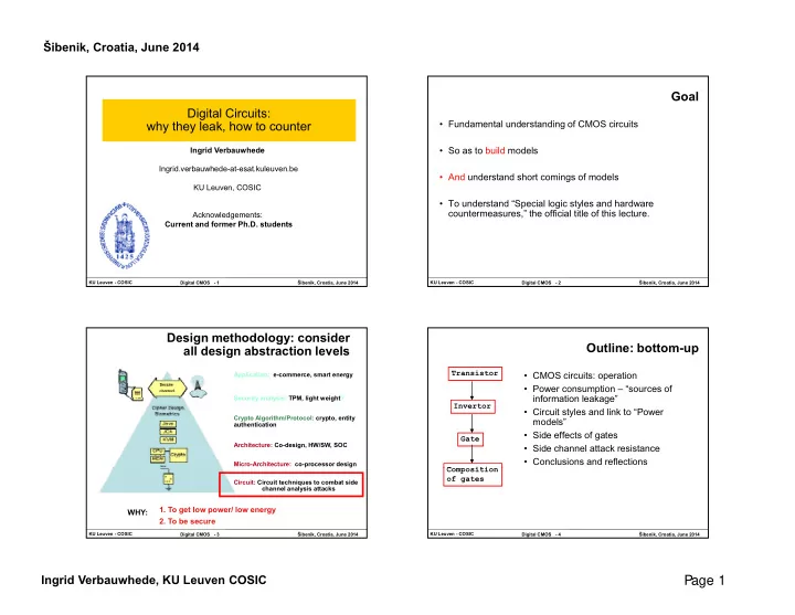
Outline: bottom-up

  • CMOS circuits: operation
  • Power consumption – “sources of

information leakage”

Transistor

information leakage

  • Circuit styles and link to “Power

models”

  • Side effects of gates
  • Side channel attack resistance
  • Conclusions and reflections

Invertor Gate Composition

KU Leuven - COSIC Digital CMOS - 4 Šibenik, Croatia, June 2014

Composition

  • f gates
slide-2
SLIDE 2

Šibenik, Croatia, June 2014

Page 2

Ingrid Verbauwhede, KU Leuven COSIC Outline

  • CMOS circuits: operation
  • Power consumption – “sources of

information leakage”

Transistor

information leakage

– Current – Dynamic power – Static power

Invertor

KU Leuven - COSIC Digital CMOS - 5 Šibenik, Croatia, June 2014

CMOS invertor

power and energy fundamentals

KU Leuven - COSIC Digital CMOS - 6 Šibenik, Croatia, June 2014

The CMOS Inverter: A First Glance

VDD Vin Vout CL

KU Leuven - COSIC Digital CMOS - 7 Šibenik, Croatia, June 2014 Slide courtesy: J. Rabaey

The image cannot be displayed. Your computer may not have enough memory to open the image, or the image may have been corrupted. Restart your computer, and then open the file again. If the red x still appears, you may have to delete the image and then insert it again.

CMOS Inverter

VDD PMOS 2

VDD

N Well Polysilicon In Out Metal 1

Out In PMOS NMOS

Contacts

KU Leuven - COSIC Digital CMOS - 8 Šibenik, Croatia, June 2014

GND NMOS

Slide courtesy: J. Rabaey

slide-3
SLIDE 3

Šibenik, Croatia, June 2014

Page 3

Ingrid Verbauwhede, KU Leuven COSIC Two Inverters

Share power and ground LEGO style: Abut cells

Connect in Metal

LEGO style: Abut cells

VDD

KU Leuven - COSIC Digital CMOS - 9 Šibenik, Croatia, June 2014 Slide courtesy: J. Rabaey

AC/DC of CMOS Inverter: DC

VDD VDD = STATIC behavior

VOL = 0 VOH = VDD

Vout Vout Rn Rp

KU Leuven - COSIC Digital CMOS - 10 Šibenik, Croatia, June 2014

Vin = VDD Vin = 0

n

Slide courtesy: J. Rabaey

Why we like CMOS!!

  • Full swing
  • NO DC current!!*

*to first order, see further

AC/DC of CMOS Inverter: AC

V DD V DD = DYNAMIC behavior

tpHL = f(Ron.CL) = 0.69 RonCL

V out R n CL V out R p CL

KU Leuven - COSIC Digital CMOS - 11 Šibenik, Croatia, June 2014

R n V in = V DD (b) High-to-low V in = 0 (a) Low-to-high

Slide courtesy: J. Rabaey

SPA, DPA attack AC!!

Where Does Power Go in CMOS?

  • Dynamic Power Consumption = AC
  • Charging and discharging capacitors

Charging and discharging capacitors

  • [Short Circuit Currents = AC]
  • Short circuit path between supply rails during

switching

  • No longer an issue in deep submicron

KU Leuven - COSIC Digital CMOS - 12 Šibenik, Croatia, June 2014

  • Leakage = DC
  • Leaking diodes and transistors
slide-4
SLIDE 4

Šibenik, Croatia, June 2014

Page 4

Ingrid Verbauwhede, KU Leuven COSIC AC – Dynamic Power consumption

Vdd Vin Vout

C

L

Energy/transition = CL * Vdd

2 * α

KU Leuven - COSIC Digital CMOS - 13 Šibenik, Croatia, June 2014

Power = Energy/transition * f = CL * Vdd

2

* f

  • Energy = independent of clock frequency!
  • Energy = depends on activity α !
  • Energy, power = independent of transistor sizes
  • Need to reduce CL, Vdd, α and f to reduce power

* α

AC – SPA, DPA

  • SPA and DPA monitor power
  • Which values depend on data?

– Monitor α, the activity of circuit – Monitor CL, the capacitance

  • Hamming weight:

– Measures activity between current and (past) known value – Typically for pre-charged values

  • Hamming Distance:

KU Leuven - COSIC Digital CMOS - 14 Šibenik, Croatia, June 2014

g

– Measures activity between current and previous value – Typical for standard cell based design – Also for FPGA

Example: power model bus

  • 8 bit bus on a smart card, pre-charged
  • (relatively) large capacitance
  • Hamming weight model

= numbers of bits set to 1

Side-note: on a pre-charged bus which is pre-set to 1 maximum power

KU Leuven - COSIC Digital CMOS - 15 Šibenik, Croatia, June 2014

Side note: on a pre charged bus which is pre set to 1, maximum power consumption is for data all zero.

CPA – Hamming Weight model

KU Leuven - COSIC Digital CMOS - 16 Šibenik, Croatia, June 2014

slide-5
SLIDE 5

Šibenik, Croatia, June 2014

Page 5

Ingrid Verbauwhede, KU Leuven COSIC AC - Correlation Power Analysis

  • R := reference state

– Which bit pattern was previously present? E.g. A h d l A pre-charged value An opcode on the bus A previously stored value in a register

  • Power model:

b R k x SBox HW a

i

     ) ) ( (

KU Leuven - COSIC Digital CMOS - 17 Šibenik, Croatia, June 2014

a,b are constant, linear model HW is defined as Hamming Weight = counts number of 1’s.

DC

leakage currents as Side-channel information leakage

KU Leuven - COSIC Digital CMOS - 18 Šibenik, Croatia, June 2014

Side channel information leakage

DC - Leakage current

V V V DD

Problem in deep submicron (below 45 nm)

V in V out

Drain Junction leakage Subthreshold current

KU Leuven - COSIC Digital CMOS - 19 Šibenik, Croatia, June 2014

Problem in deep submicron (below 45 nm) Depends strongly on “threshold voltage” Vt

  • Vt is set by processing
  • “High Vt” “low Vt” Standard cell library
  • Low power FPGAs vs High performance FPGAs

Vt and Vdd effect on leakage

  • Vt, Vdd combination for low power, given a target clock frequency

Power [arb. Unit] Leakage Dynamic Total VDD [V] VDD [V]

KU Leuven - COSIC Digital CMOS - 20 Šibenik, Croatia, June 2014

Memory → Leakage dominance High performance microprocessor → dynamic power dominance

DD [ ]

10x more switching

[slide credit: Wim Dehaene]

slide-6
SLIDE 6

Šibenik, Croatia, June 2014

Page 6

Ingrid Verbauwhede, KU Leuven COSIC DC – leakage of NAND gate

A=0 B=Vdd A=Vdd B=0 A=0 B=0 Vdd Vdd Vdd Nand gate: out = ‘1’ but I1 ≠ I2 ≠ I3 I1 I2 I3

KU Leuven - COSIC Digital CMOS - 21 Šibenik, Croatia, June 2014

Nand gate: out = 1 , but I1 ≠ I2 ≠ I3

  • New source of information,
  • Available even when device is at ‘rest’
  • Time window to attack larger
  • Less a problem for memory because differential structure

If you are looking for a nice research topic.

Outline

  • CMOS circuits: operation
  • Power consumption – “sources of leakage”
  • Circuit styles and link to “Power models”

Transistor

  • Circuit styles and link to Power models

– Static CMOS – Dynamic, pre-charged CMOS – Differential CMOS – Dynamic – differential CMOS – Link to Hamming Weight – Hamming Distance

  • Side effects of gates
  • Side channel attack resistance

Gate Invertor Gate

KU Leuven - COSIC Digital CMOS - 22 Šibenik, Croatia, June 2014

  • Conclusions and reflections

Static CMOS

Basics and construction rules

KU Leuven - COSIC Digital CMOS - 23 Šibenik, Croatia, June 2014

Standard cell automated design flow

HDL HDL Behavioral Behavioral Design Capture Logic Synthesis Logic Synthesis Floorplanning Floorplanning Placement Placement Pre-Layout Simulation Pre-Layout Simulation Post-Layout Simulation Post-Layout Simulation Structural Structural Physical Physical Design Iteration Design Iteration

KU Leuven - COSIC Digital CMOS - 24 Šibenik, Croatia, June 2014

Routing Routing Tape-out Circuit Extraction Circuit Extraction y

Timing closure!

Technology/library/manufacturer input

slide-7
SLIDE 7

Šibenik, Croatia, June 2014

Page 7

Ingrid Verbauwhede, KU Leuven COSIC Standard Cell Zoom In

layout

vdd vss

KU Leuven - COSIC Digital CMOS - 25 Šibenik, Croatia, June 2014

y

KU Leuven - COSIC Digital CMOS - 26 Šibenik, Croatia, June 2014

More levels of metal: top levels not shown

Glitches in static CMOS networks

A B X Z C ABC X Z 101 000 C

[MJI] Glitch

C X

KU Leuven - COSIC Digital CMOS - 27 Šibenik, Croatia, June 2014

Unit Delay

Glitch = Useless transition = Waste of energy [Low Power community has addressed this]

Most famous example: RippleCarry Adder

Add0 Add1 Add2 Add14 Add15 C

4.0

Voltage, Volts

S15 6 4

Add0 Add1 Add2 Add14 Add15 S0 S1 S2 S14 S15 Cin

KU Leuven - COSIC Digital CMOS - 28 Šibenik, Croatia, June 2014 5 10 0.0 2.0

Time, ns Sum Output

Cin S10 5 3 2 S1 From From Rabaey Rabaey, , 1995 1995 Design for low power Design for low power

slide-8
SLIDE 8

Šibenik, Croatia, June 2014

Page 8

Ingrid Verbauwhede, KU Leuven COSIC Glitch Reduction: Path balancing

  • Avoids glitching: general design practice for low power technique
  • Principle: transform algorithm into tree like structure
  • Then balance delay paths in all paths to output
  • Examples:

– Log adder replaces Ripple Adder – Wallace tree replaces Carry-Save multiplier

  • Synthesis tools will transform for you “automatically”.

KU Leuven - COSIC Digital CMOS - 29 Šibenik, Croatia, June 2014

Dynamic CMOS

Basics and construction rules

KU Leuven - COSIC Digital CMOS - 30 Šibenik, Croatia, June 2014

Dynamic CMOS

  • In static circuits at every point in time (except when

switching) the output is connected to either GND or VDD via a low resistance path a low resistance path.

– fan-in of n requires 2n (n N-type + n P-type) devices

  • Dynamic circuits rely on the temporary storage of signal

values on the capacitance of high impedance nodes.

– requires on n + 2 (n+1 N-type + 1 P-type) transistors

KU Leuven - COSIC Digital CMOS - 31 Šibenik, Croatia, June 2014

Dynamic Gate

Mp

Clk Clk

Mpon

1

  • ff

In1 In2 PDN In3

Me

p

Clk Out CL Out A B C

pon

  • ff

1 ((AB)+C)

KU Leuven - COSIC Digital CMOS - 32 Šibenik, Croatia, June 2014

Clk

Me

Two phase operation Precharge (Clk = 0) Evaluate (Clk = 1)

  • n
slide-9
SLIDE 9

Šibenik, Croatia, June 2014

Page 9

Ingrid Verbauwhede, KU Leuven COSIC Conditions on Output

  • Once the output of a dynamic gate is discharged, it cannot

be charged again until the next precharge operation. Inputs to the gate can make at most one transition during

  • Inputs to the gate can make at most one transition during

evaluation.

  • Output can be in the high impedance state during and after

evaluation (PDN off), state is stored on CL Thus by construction dynamic gates cannot glitch!

KU Leuven - COSIC Digital CMOS - 33 Šibenik, Croatia, June 2014

Thus by construction, dynamic gates cannot glitch!

Circuits against side channel attacks

How they leak How to solve it

KU Leuven - COSIC Digital CMOS - 34 Šibenik, Croatia, June 2014

How to solve it

Remember AC – SPA, DPA

Energy/transition = CL * Vdd

2 * α

Power = Energy/transition * f = CL * Vdd

2

* f * α

  • SPA and DPA monitor power
  • Address α, CL

– Monitor α, the activity of circuit – Monitor CL, the capacitance

KU Leuven - COSIC Digital CMOS - 35 Šibenik, Croatia, June 2014

Transition independent power consumption …

  • …doesn’t create any side channel information
  • No Hamming distance, No Hamming weight
  • When logic values are measured by charging and

discharging capacitances, we need to use a fixed amount of energy for every transition switch once

KU Leuven - COSIC Digital CMOS - 36 Šibenik, Croatia, June 2014

switch once every cycle switch a constant load capacitance CL = constant α = 1

slide-10
SLIDE 10

Šibenik, Croatia, June 2014

Page 10

Ingrid Verbauwhede, KU Leuven COSIC Dynamic and differential logic

  • Dynamic & differential

– α = 1 – No glitches

  • Differential (with design effort):

– CL is constant – Also includes differential routing – Static Leakage current is data independent

KU Leuven - COSIC Digital CMOS - 37 Šibenik, Croatia, June 2014

Solution based on Standard cells

B A Z

A

Z B A Z

2

  • false output

B A B B Z A B prch Z B Z

De-Morgan’s Law AND-ing with precharge signal 1

  • precharge 1:

t t

KU Leuven - COSIC Digital CMOS - 38 Šibenik, Croatia, June 2014

  • with false inputs
  • utputs are 0
  • precharge 0 - evaluation:

1 output is 1

Wave Dynamic Differential Logic

  • 0-wave travels from input to output during pre-charge

– input 0  output 0 – no pre-charge operator

Differential data travels during evaluation

  • Differential data travels during evaluation

AND gate OR t precharge inputs register

KU Leuven - COSIC Digital CMOS - 39 Šibenik, Croatia, June 2014

OR gate prch clk Encryption Module clk

eval. prch.

[Tiri,DATE2004]

  • All functions of and2, or2 operator
  • In addition: inverted input, output signals
  • XOR2X4:

OAI221X2:

WDDL library

  • XOR2X4:

OAI221X2:

  • Our WDDL library: 128 cells

A

A Y

AOI22X1 INVX4

C0

OAI221X1 AOI221X1

A0 A1 B0 B1 Y

INVX2 INVX2

A0 KU Leuven - COSIC Digital CMOS - 40 Šibenik, Croatia, June 2014 B B Y

OAI22X1 INVX4

Y A1 B0 B1 C0

slide-11
SLIDE 11

Šibenik, Croatia, June 2014

Page 11

Ingrid Verbauwhede, KU Leuven COSIC Unbalanced capacitive loads

  • For constant power consumption:

constant load capacitance.

  • Match loads at differential outputs
  • Match loads at differential outputs.

KU Leuven - COSIC Digital CMOS - 41 Šibenik, Croatia, June 2014

Load capacitance breakdown

Ci,I1 Rw,A’ Cw,A Rw,A

  • Intrinsic caps.:

matched I t t

Co,A’ Co,A Ci,I2 Ci,I1’ gate gate 2 gate 1 Co: intrinsic output capacitance Cw,A’

  • Interconnect:

dominant (Moore’s law)

  • Balancing

interconnect: crucial

KU Leuven - COSIC Digital CMOS - 42 Šibenik, Croatia, June 2014

CA = CA’ Co,A + Cw,A + Ci,I1 + … Ci,Ik = Co,A’ + Cw,A’ + Ci,I1’ + … Ci,Ik’ Cw,A = Cw,A’

Ci,I2’ Co: intrinsic output capacitance Cw: interconnect capacitance Ci: input capacitance

Design example

KU Leuven - COSIC Digital CMOS - 43 Albena, July 2013

43

  • Two normal wires replace each fat wire.

WDDL Example

  • Same circuit; two implementations.

– Insecure reference design – Secure design

WDDL differential route single ended regular route

KU Leuven - COSIC Digital CMOS - 44 Šibenik, Croatia, June 2014

slide-12
SLIDE 12

Šibenik, Croatia, June 2014

Page 12

Ingrid Verbauwhede, KU Leuven COSIC Early propagation effect

  • Static CMOS, dynamic CMOS, differential CMOS,
  • Timing of transition is data dependent

A A B B C C Out Out

A B C D O T1 T2

D D

KU Leuven - COSIC Digital CMOS - 45 Šibenik, Croatia, June 2014

Pre Eval 1 X X X @T1 0 @T1 2 Eval 2 1 0 @T1 0 @T2 1 1 Eval 3 1 1 1 @T1 1 @T2 1 1

Early propagation effect: balance

A A B B Out Out C C

A B C D O T1 T2 Pre Eval 1 X X X @T1 0 @T2 1 1

KU Leuven - COSIC Digital CMOS - 46 Šibenik, Croatia, June 2014

Eval 2 1 0 @T1 0 @T2 1 1 Eval 3 1 1 1 @T1 1 @T2 1 1

Can prove that it is always possible to balance in WDDL logic.

script lib.v

Integration in standard cell design flow: Secure digital design

logic synthesis logic design behavior.v design specs rtl.v cell substitution fat_lib.lef diff_lib.lef place interconnect stream

KU Leuven - COSIC Digital CMOS - 47 Šibenik, Croatia, June 2014

& route fat.v fat.def interconnect decomposition diff.def layout stream

  • ut

Few key modifications with minimal influence in backend of regular synchronous static CMOS standard cell design flow

[Tiri,TCAD2006]

Conclusions and reflections

  • Fundamental understanding CMOS circuits

– AC DC behavior – Static CMOS: low power but shows Hamming distance

Transistor

Static CMOS: low power, but shows Hamming distance – Dynamic CMOS: high speed, no glitches, but shows Hamming weight – Dynamic, differential: hides data dependencies – Full custom style: SABL – Standard cell compatible: WDDL (with construction rules)

  • Side effect of CMOS gates:

– Glitch: only problem of static CMOS

Invertor Gate

KU Leuven - COSIC Digital CMOS - 48 Šibenik, Croatia, June 2014

Glitch: only problem of static CMOS – Memory effect: static CMOS – Early propagation: can be addressed in WDDL

  • Future: address DC leakage current

– Leakage even when there is no operation

Composition

  • f gates