Multicycle Approach CSE 675.02: Introduction to Computer - - PowerPoint PPT Presentation

multicycle approach
SMART_READER_LITE
LIVE PREVIEW

Multicycle Approach CSE 675.02: Introduction to Computer - - PowerPoint PPT Presentation

Multicycle Approach CSE 675.02: Introduction to Computer Architecture We will be reusing functional units Designing ALU used to compute address and to increment PC MIPS Processor Memory used for instruction and data Our


slide-1
SLIDE 1

08/08/2005

Designing MIPS Processor

(Multi-Cycle)

Presentation H CSE 675.02: Introduction to Computer Architecture

Slides by Gojko Babić and Elsevier Publishing

  • We will be reusing functional units

– ALU used to compute address and to increment PC – Memory used for instruction and data

  • Our control signals will not be determined

directly by instruction

– e.g., what should the ALU do for a “subtract” instruction?

  • We’ll use a finite state machine for control
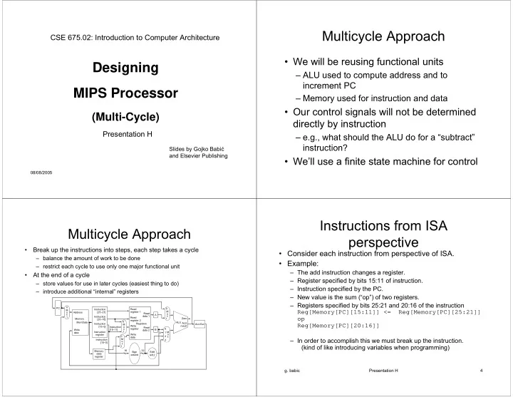
Multicycle Approach

  • Break up the instructions into steps, each step takes a cycle

– balance the amount of work to be done – restrict each cycle to use only one major functional unit

  • At the end of a cycle

– store values for use in later cycles (easiest thing to do) – introduce additional “internal” registers

Multicycle Approach

Read register 1 Read register 2 Write register Write data Registers ALU Zero Read data 1 Read data 2 Sign extend 16 32 Instruction [25–21] Instruction [20–16] Instruction [15–0] ALU result M u x M u x Shift left 2 Instruction register PC 1 M u x 1 M u x 1 M u x 1 A B 1 2 3 ALUOut Instruction [15–0] Memory data register Address Write data Memory MemData 4 Instruction [15–11]

  • g. babic

Presentation H 4

Instructions from ISA perspective

  • Consider each instruction from perspective of ISA.
  • Example:

– The add instruction changes a register. – Register specified by bits 15:11 of instruction. – Instruction specified by the PC. – New value is the sum (“op”) of two registers. – Registers specified by bits 25:21 and 20:16 of the instruction Reg[Memory[PC][15:11]] <= Reg[Memory[PC][25:21]]

  • p

Reg[Memory[PC][20:16]] – In order to accomplish this we must break up the instruction. (kind of like introducing variables when programming)

slide-2
SLIDE 2
  • g. babic

Presentation H 5

Breaking down an instruction

  • ISA definition of arithmetic:

Reg[Memory[PC][15:11]] <= Reg[Memory[PC][25:21]] op Reg[Memory[PC][20:16]]

  • Could break down to:

– IR <= Memory[PC] – A <= Reg[IR[25:21]] – B <= Reg[IR[20:16]] – ALUOut <= A op B – Reg[IR[20:16]] <= ALUOut

  • We forgot an important part of the definition of arithmetic!

– PC <= PC + 4

  • g. babic

Presentation H 6

Idea behind multicycle approach

  • We define each instruction from the ISA perspective (do this!)
  • Break it down into steps following our rule that data flows through at

most one major functional unit (e.g., balance work across steps)

  • Introduce new registers as needed (e.g, A, B, ALUOut, MDR, etc.)
  • Finally try and pack as much work into each step

(avoid unnecessary cycles) while also trying to share steps where possible (minimizes control, helps to simplify solution)

  • Result: Our book’s multicycle Implementation!
  • Instruction Fetch
  • Instruction Decode and Register Fetch
  • Execution, Memory Address Computation, or Branch

Completion

  • Memory Access or R-type instruction completion
  • Write-back step

INSTRUCTIONS TAKE FROM 3 - 5 CYCLES!

Five Execution Steps

  • Use PC to get instruction and put it in the Instruction

Register.

  • Increment the PC by 4 and put the result back in the PC.
  • Can be described succinctly using RTL "Register-Transfer

Language" IR <= Memory[PC]; PC <= PC + 4; Can we figure out the values of the control signals? What is the advantage of updating the PC now?

Step 1: Instruction Fetch

slide-3
SLIDE 3
  • Read registers rs and rt in case we need them
  • Compute the branch address in case the instruction is a

branch

  • RTL:

A <= Reg[IR[25:21]]; B <= Reg[IR[20:16]]; ALUOut <= PC + (sign-extend(IR[15:0]) << 2);

  • We aren't setting any control lines based on the

instruction type (we are busy "decoding" it in our control logic)

Step 2: Instruction Decode and Register Fetch

  • ALU is performing one of three functions, based on

instruction type

  • Memory Reference:

ALUOut <= A + sign-extend(IR[15:0]);

  • R-type:

ALUOut <= A op B;

  • Branch:

if (A==B) PC <= ALUOut;

Step 3 (instruction dependent)

  • Loads and stores access memory

MDR <= Memory[ALUOut];

  • r

Memory[ALUOut] <= B;

  • R-type instructions finish

Reg[IR[15:11]] <= ALUOut; The write actually takes place at the end of the cycle on the edge

Step 4 (R-type or memory- access)

  • Reg[IR[20:16]] <= MDR;

Which instruction needs this?

Write-back step

slide-4
SLIDE 4

Summary:

  • How many cycles will it take to execute this code?

lw $t2, 0($t3) lw $t3, 4($t3) beq $t2, $t3, Label #assume not add $t5, $t2, $t3 sw $t5, 8($t3) Label: ...

  • What is going on during the 8th cycle of execution?
  • In what cycle does the actual addition of $t2 and $t3 takes

place?

Simple Questions

  • g. babic

Presentation H 15

Read register 1 Read register 2 Write register Write data Registers ALU Zero Read data 1 Read data 2 Sign extend 16 32 Instruction [31–26] Instruction [25–21] Instruction [20–16] Instruction [15–0] ALU result M u x M u x Shift left 2 Shift left 2 Instruction register PC 1 M u x 1 M u x 1 M u x 1 A B 1 2 3 M u x 1 2 ALUOut Instruction [15–0] Memory data register Address Write data Memory MemData 4 Instruction [15–11] PCWriteCond PCWrite IorD MemRead MemWrite MemtoReg IRWrite PCSource ALUOp ALUSrcB ALUSrcA RegWrite RegDst 26 28 Outputs Control Op [5–0] ALU control PC [31–28] Instruction [25-0] Instruction [5–0] Jump address [31–0]

  • Finite state machines:

– a set of states and – next state function (determined by current state and the input) – output function (determined by current state and possibly input) – We’ll use a Moore machine (output based only on current state)

Review: finite state machines

Inputs Current state Outputs Clock Next-state function Output function Next state

slide-5
SLIDE 5

Review: finite state machines

  • Example:
  • B. 37 A friend would like you to build an “electronic eye” for

use as a fake security device. The device consists of three lights lined up in a row, controlled by the outputs Left, Middle, and Right, which, if asserted, indicate that a light should be

  • n. Only one light is on at a time, and the light “moves” from

left to right and then from right to left, thus scaring away thieves who believe that the device is monitoring their activity. Draw the graphical representation for the finite state machine used to specify the electronic eye. Note that the rate of the eye’s movement will be controlled by the clock speed (which should not be too great) and that there are essentially no inputs.

  • Value of control signals is dependent upon:

– what instruction is being executed – which step is being performed

  • Use the information we’ve accumulated to specify a

finite state machine

– specify the finite state machine graphically, or – use microprogramming

  • Implementation can be derived from specification

Implementing the Control

  • g. babic

Presentation H 19

Finite State Machines Introduction

  • g. babic

Presentation H 20

Finite State Machine Example: 3 ones…

Draw the FSM…

1 00 1 10 00 10 10 1 01 00 01 01 1 00 00 00 Output NS Input PS

Truth table…

slide-6
SLIDE 6
  • g. babic

Presentation H 21

Hardware Implementation of FSM

+ = ?

  • g. babic

Presentation H 22

  • A current state is kept in the Current state register.
  • Next state function is determined by current state and the input.
  • Output function is determined by current state and input.
  • We will use a Moore machine, where output is based only on

current state.

N e xt-state func tio n C u rre nt state C lock O u tp ut func tio n N e xt state O utpu ts Inp uts

Finite State Machines

Figure B.10.1

  • g. babic

Presentation H 23

Finite State Machine Graph for Control Unit

PCW rite PC Source = 10 ALUSrcA = 1 ALUSrcB = 00 ALUO p = 01 PC W riteCond PC Source = 01 ALUSrcA = 1 ALUSrcB = 00 ALUO p = 10 RegD st = 1 RegW rite M em toReg = 0 M em W rite IorD = 1 Mem Read IorD = 1 ALUSrcA = 1 ALUSrcB = 10 ALUOp = 00 R egDst = 0 RegW rite M em toR eg = 1 ALUSrcA = 0 ALUSrcB = 11 ALUO p = 00 M em R ead ALUSrcA = 0 IorD = 0 IRW rite ALUSrcB = 01 ALUO p = 00 PCW rite PC Source = 00 Instruction fetch Instruction decode/ register fetch Jump completion Branch com pletion Execution M emory address com putation M emory access M em ory access R-type com pletion W rite-back step (Op = 'LW ') or (Op = 'SW ') (Op = R-type) ( O p = ' B E Q ' ) (Op = 'J') (Op = 'SW') (Op = 'LW') 4 1 9 8 6 2 7 5 3 Start

ALUSrcA=0 ALUSrcB=01 ALUOp=01

Figure 5.38

with corrections in red

  • Note:

– don’t care if not mentioned – asserted if name only – otherwise exact value

  • How many state

bits will we need?

Graphical Specification

  • f FSM

MemRead ALUSrcA = 0 IorD = 0 IRWrite ALUSrcB = 01 ALUOp = 00 PCWrite PCSource = 00 ALUSrcA = 0 ALUSrcB = 11 ALUOp = 00 ALUSrcA = 1 ALUSrcB = 00 ALUOp = 10 ALUSrcA = 1 ALUSrcB = 10 ALUOp = 00 MemRead IorD = 1 MemWrite IorD = 1 RegDst = 1 RegWrite MemtoReg = 0 RegDst = 1 RegWrite MemtoReg = 0 PCWrite PCSource = 10 ALUSrcA = 1 ALUSrcB = 00 ALUOp = 01 PCWriteCond PCSource = 01 Instruction decode/ register fetch Instruction fetch 1 Start Jump completion 9 8 6 2 3 4 5 7 Memory read completon step R-type completion Memory access Memory access Execution Branch completion Memory address computation

slide-7
SLIDE 7
  • g. babic

Presentation H 25

  • Use PC to get instruction and put it in the Instruction Register,

i.e. IR Memory[PC];

  • Increment the PC by 4 and put the result back in the PC,

i.e. PC [PC] + 4;

  • Can we figure out the values of the control signals?
  • Here are rules for signals that are omitted:

– If signal for mux is not stated, it is don’t care – If ALU signals are not stated, they are don’t care – If MemRead, MemWrite, RegWrite, IRWrite, PCWrite or PCWriteCond is not stated, it is unasserted, i.e. logical 0.

Step 1: Instruction Fetch

IorD=0, MemRead, IRWrite ALUSrcA=0, ALUSrcB=01, ALUOp=00, PCSource=0, PCWrite

  • g. babic

Presentation H 26

  • We aren't setting any control lines based on the instruction type

(we are busy "decoding" it in our control logic)

  • Read registers rs and rt in case we need them:

A Reg[IR[25-21]]; B Reg[IR[20-16]]; Done automatically

  • Compute the branch address in case the instruction is a

branch: ALUOut PC + (sign-extend(IR[15-0]) << 2); ALUSrcA=0, ALUSrcB=11, ALUOp=00

Step 2: Instruction Decode & Register Fetch

  • g. babic

Presentation H 27

  • ALU is performing one of three functions, based on

instruction type

  • Memory Reference (lw or sw):

ALUOut A + sign-extend(IR[15-0]);

  • R-type:

ALUOut A op B;

  • Branch on Equal:

if (A==B) PC ALUOut;

Step 3: Instruction Dependent

ALUSrcA=1, ALUSrcB=10, ALUop=00 ALUSrcA=1, ALUSrcB=00, ALU0p=10 ALUSrcA=1, ALUSrcB=00, ALU0p=01 PCSource=01, PCWriteCond Note: beq instruction is done, thus this instruction requires 3 clock cycles to execute.

  • g. babic

Presentation H 28

  • Step 4: R-type and Memory Access

– Loads and stores access memory MDR Memory[ALUOut] (load);

  • r

Memory[ALUOut] B (store); – R-type instructions finish Reg[IR[15-11]] ALUOut; Register write actually takes place at the end of the cycle

  • n the falling edge

– Store and R-type instructions are done in 4 clock cycles

  • Step 5: Write back (load only)

– Reg[IR[20-16]] MDR

Steps 4 and 5: Instruction Dependent

IorD=1, MemRead IorD=1, MemWrite RegDst=1, MemToReg=0, RegWrite RegDst=0, MemToReg=1, RegWrite

slide-8
SLIDE 8
  • g. babic

Presentation H 29

Step name Action for R-type instructions Action for memory-reference instructions Action for branches Action for jumps Instruction fetch IR Memory[PC] PC PC + 4 Instruction A Reg [IR[25-21]] decode/register fetch B Reg [IR[20-16]] ALUOut PC + (sign-extend (IR[15-0]) << 2) Execution, address ALUOut A op B ALUOut A + sign-extend if (A ==B) then PC PC [31-28] II computation, branch/ (IR[15-0]) PC ALUOut (IR[25-0]<<2) jump completion Memory access or R-type Reg [IR[15-11]] Load: MDRMemory[ALUOut] completion ALUOut

  • r

Store: Memory [ALUOut]B Memory read completion Load: Reg[IR[20-16]] MDR

Summary of Instruction Executions

Note: Jump instruction added: PCSource=10, PCWrite

Figure 5.50

  • Implementation:

Finite State Machine for Control

PCWrite PCWriteCond IorD MemtoReg PCSource ALUOp ALUSrcB ALUSrcA RegWrite RegDst NS3 NS2 NS1 NS0 Op5 Op4 Op3 Op2 Op1 Op0 S3 S2 S1 S0 State register IRWrite MemRead MemWrite Instruction register

  • pcode field

Outputs Control logic Inputs

PLA Implementation

Op5 Op4 Op3 Op2 Op1 Op0 S3 S2 S1 S0 IorD IRWrite MemRead MemWrite PCWrite PCWriteCond MemtoReg PCSource1 ALUOp1 ALUSrcB0 ALUSrcA RegWrite RegDst NS3 NS2 NS1 NS0 ALUSrcB1 ALUOp0 PCSource0

  • ROM = "Read Only Memory"

– values of memory locations are fixed ahead of time

  • A ROM can be used to implement a truth table

– if the address is m-bits, we can address 2m entries in the ROM. – our outputs are the bits of data that the address points to. m is the "height", and n is the "width"

ROM Implementation

m n

0 0 0 0 0 1 1 0 0 1 1 1 0 0 0 1 0 1 1 0 0 0 1 1 1 0 0 0 1 0 0 0 0 0 0 1 0 1 0 0 0 1 1 1 0 0 1 1 0 1 1 1 0 1 1 1

slide-9
SLIDE 9
  • How many inputs are there?

6 bits for opcode, 4 bits for state = 10 address lines (i.e., 210 = 1024 different addresses)

  • How many outputs are there?

16 datapath-control outputs, 4 state bits = 20 outputs

  • ROM is 210 x 20 = 20K bits (and a rather unusual size)
  • Rather wasteful, since for lots of the entries, the outputs

are the same — i.e., opcode is often ignored

ROM Implementation

  • Break up the table into two parts

— 4 state bits tell you the 16 outputs, 24 x 16 bits of ROM — 10 bits tell you the 4 next state bits, 210 x 4 bits of ROM — Total: 4.3K bits of ROM

  • PLA is much smaller

— can share product terms — only need entries that produce an active output — can take into account don't cares

  • Size is (#inputs × #product-terms) + (#outputs × #product-terms)

For this example = (10x17)+(20x17) = 510 PLA cells

  • PLA cells usually about the size of a ROM cell (slightly bigger)

ROM vs PLA

  • Complex instructions: the "next state" is often

current state + 1

Another Implementation Style

AddrCtl Outputs PLA or ROM State Address select logic Op[5– 0] Adder Instruction register

  • pcode field

1 Control unit Input PCWrite PCWriteCond IorD MemtoReg PCSource ALUOp ALUSrcB ALUSrcA RegWrite RegDst IRWrite MemRead MemWrite BWrite

Details

Dispatch ROM 1 Dispatch ROM 2 Op Opcode name Value Op Opcode name Value 000000 R-format 0110 100011 lw 0011 000010 jmp 1001 101011 sw 0101 000100 beq 1000 100011 lw 0010 101011 sw 0010

State number Address-control action Value of AddrCtl Use incremented state 3 1 Use dispatch ROM 1 1 2 Use dispatch ROM 2 2 3 Use incremented state 3 4 Replace state number by 0 5 Replace state number by 0 6 Use incremented state 3 7 Replace state number by 0 8 Replace state number by 0 9 Replace state number by 0

State Adder 1 PLA or ROM Mux 3 2 1 Dispatch ROM 1 Dispatch ROM 2 AddrCtl Address select logic Instruction register

  • pcode field
slide-10
SLIDE 10

Microprogramming

PCWrite PCWriteCond IorD MemtoReg PCSource ALUOp ALUSrcB ALUSrcA RegWrite AddrCtl Outputs Microcode memory IRWrite MemRead MemWrite RegDst Control unit Input Microprogram counter Address select logic Adder 1 Instruction register

  • pcode field

BWrite Datapath

  • A specification methodology

– appropriate if hundreds of opcodes, modes, cycles, etc. – signals specified symbolically using microinstructions

  • Will two implementations of the same architecture have the

same microcode?

  • What would a microassembler do?

Microprogramming

Label ALU control SRC1 SRC2 Register control Memory PCWrite control Sequencing Fetch Add PC 4 Read PC ALU Seq Add PC Extshft Read Dispatch 1 Mem1 Add A Extend Dispatch 2 LW2 Read ALU Seq Write MDR Fetch SW2 Write ALU Fetch Rformat1 Func code A B Seq Write ALU Fetch BEQ1 Subt A B ALUOut-cond Fetch JUMP1 Jump address Fetch

Microinstruction format

Field name Value Signals active Comment Add ALUOp = 00 Cause the ALU to add. ALU control Subt ALUOp = 01 Cause the ALU to subtract; this implements the compare for branches. Func code ALUOp = 10 Use the instruction's function code to determine ALU control. SRC1 PC ALUSrcA = 0 Use the PC as the first ALU input. A ALUSrcA = 1 Register A is the first ALU input. B ALUSrcB = 00 Register B is the second ALU input. SRC2 4 ALUSrcB = 01 Use 4 as the second ALU input. Extend ALUSrcB = 10 Use output of the sign extension unit as the second ALU input. Extshft ALUSrcB = 11 Use the output of the shift-by-two unit as the second ALU input. Read Read two registers using the rs and rt fields of the IR as the register numbers and putting the data into registers A and B. Write ALU RegWrite, Write a register using the rd field of the IR as the register number and Register RegDst = 1, the contents of the ALUOut as the data. control MemtoReg = 0 Write MDR RegWrite, Write a register using the rt field of the IR as the register number and RegDst = 0, the contents of the MDR as the data. MemtoReg = 1 Read PC MemRead, Read memory using the PC as address; write result into IR (and lorD = 0 the MDR). Memory Read ALU MemRead, Read memory using the ALUOut as address; write result into MDR. lorD = 1 Write ALU MemWrite, Write memory using the ALUOut as address, contents of B as the lorD = 1 data. ALU PCSource = 00 Write the output of the ALU into the PC. PCWrite PC write control ALUOut-cond PCSource = 01, If the Zero output of the ALU is active, write the PC with the contents PCWriteCond

  • f the register ALUOut.

jump address PCSource = 10, Write the PC with the jump address from the instruction. PCWrite Seq AddrCtl = 11 Choose the next microinstruction sequentially. Sequencing Fetch AddrCtl = 00 Go to the first microinstruction to begin a new instruction. Dispatch 1 AddrCtl = 01 Dispatch using the ROM 1. Dispatch 2 AddrCtl = 10 Dispatch using the ROM 2.

  • No encoding:

– 1 bit for each datapath operation – faster, requires more memory (logic) – used for Vax 780 — an astonishing 400K of memory!

  • Lots of encoding:

– send the microinstructions through logic to get control signals – uses less memory, slower

  • Historical context of CISC:

– Too much logic to put on a single chip with everything else – Use a ROM (or even RAM) to hold the microcode – It’s easy to add new instructions

Maximally vs. Minimally Encoded

slide-11
SLIDE 11

Microcode: Trade-offs

  • Distinction between specification and implementation is sometimes blurred
  • Specification Advantages:

– Easy to design and write – Design architecture and microcode in parallel

  • Implementation (off-chip ROM) Advantages

– Easy to change since values are in memory – Can emulate other architectures – Can make use of internal registers

  • Implementation Disadvantages, SLOWER now that:

– Control is implemented on same chip as processor – ROM is no longer faster than RAM – No need to go back and make changes

  • g. babic

Presentation H 42

Historical Perspective

  • In the ‘60s and ‘70s microprogramming was very important for

implementing machines

  • This led to more sophisticated ISAs and the VAX
  • In the ‘80s RISC processors based on pipelining became popular
  • Pipelining the microinstructions is also possible!
  • Implementations of IA-32 architecture processors since 486 use:

– “hardwired control” for simpler instructions

(few cycles, FSM control implemented using PLA or random logic)

– “microcoded control” for more complex instructions

(large numbers of cycles, central control store)

  • The IA-64 architecture uses a RISC-style ISA and can be

implemented without a large central control store

  • g. babic

Presentation H 43

Pentium 4

  • Pipelining is important (last IA-32 without it was 80386 in 1985)
  • Pipelining is used for the simple instructions favored by compilers

“Simply put, a high performance implementation needs to ensure that the simple instructions execute quickly, and that the burden of the complexities of the instruction set penalize the complex, less frequently used, instructions”

Control Control Control Enhanced floating point and multimedia Control I/O interface Instruction cache Integer datapath Data cache Secondary cache and memory interface Advanced pipelining hyperthreading support

Chapter 6 Chapter 7

  • g. babic

Presentation H 44

Pentium 4

  • Somewhere in all that “control we must handle complex instructions
  • Processor executes simple microinstructions, 70 bits wide (hardwired)
  • 120 control lines for integer datapath (400 for floating point)
  • If an instruction requires more than 4 microinstructions to implement,

control from microcode ROM (8000 microinstructions)

  • Its complicated!
Control Control Control Enhanced floating point and multimedia Control I/O interface Instruction cache Integer datapath Data cache Secondary cache and memory interface Advanced pipelining hyperthreading support
slide-12
SLIDE 12
  • g. babic

Presentation H 45

Chapter 5 Summary

  • If we understand the instructions…

We can build a simple processor!

  • If instructions take different amounts of time, multi-cycle is better
  • Datapath implemented using:

– Combinational logic for arithmetic – State holding elements to remember bits

  • Control implemented using:

– Combinational logic for single-cycle implementation – Finite state machine for multi-cycle implementation