
SLIDE 1
Physics 460 F 2006 Lect 24 1
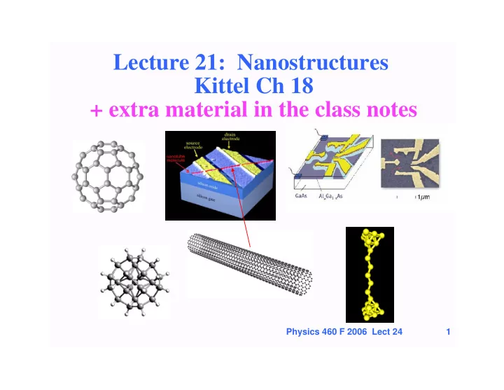
Lecture 21: Nanostructures Kittel Ch 18 + extra material in the - - PowerPoint PPT Presentation
Lecture 21: Nanostructures Kittel Ch 18 + extra material in the class notes Physics 460 F 2006 Lect 24 1 Outline Electron in a box (again) Examples of nanostructures Created by Applied Voltages Patterned metal gates on
Physics 460 F 2006 Lect 24 1
Physics 460 F 2006 Lect 24 2
Physics 460 F 2006 Lect 24 3
Physics 460 F 2006 Lect 24 4
Physics 460 F 2006 Lect 24 5
Physics 460 F 2006 Lect 24 6
Physics 460 F 2006 Lect 24 7
2 , kz = n π/L, n = 1,2, ...
Here we emphasize the case where the box is very small
Physics 460 F 2006 Lect 24 8
2 + ny 2 + nz 2 )
Physics 460 F 2006 Lect 24 9
2 + ny 2 + nz 2 )
Physics 460 F 2006 Lect 24 10
Physics 460 F 2006 Lect 24 11
Physics 460 F 2006 Lect 24 12
2 + ny 2 + nz 2 )
Physics 460 F 2006 Lect 24 13
Physics 460 F 2006 Lect 24 14
2 + ky 2 + kz 2)
Physics 460 F 2006 Lect 24 15
2 + nz 2) + ( h2/2m*) kx 2
Physics 460 F 2006 Lect 24 16
Physics 460 F 2006 Lect 24 17
Physics 460 F 2006 Lect 24 18
E kx n = 1 n = 2 E kx n = 1 n = 2
More description in Kittel Ch 18
Physics 460 F 2006 Lect 24 19
Physics 460 F 2006 Lect 24 20