Lecture 12: Sequential Networks Flip flops and registers CSE - PowerPoint PPT Presentation
Lecture 12: Sequential Networks Flip flops and registers CSE 140: Components and Design Techniques for Digital Systems Diba Mirza Dept. of Computer Science and Engineering University of California, San Diego 1 D Flip-Flop vs. D Latch
Lecture 12: Sequential Networks – Flip flops and registers CSE 140: Components and Design Techniques for Digital Systems Diba Mirza Dept. of Computer Science and Engineering University of California, San Diego 1
D Flip-Flop vs. D Latch CLK D Q D Q Q Q CLK D Q (latch) Q (flop) 2
D Flip-Flop (Delay) Id D Q(t) Q(t+1) Q D 0 0 0 0 1 0 1 0 CLK 2 1 0 1 Q’ 3 1 1 1 State table Characteristic Expression Q(t+1) = D(t) PS D 0 1 0 0 1 What does the equation mean? 1 0 1 NS= Q(t+1) 3
iClicker How long does a D-flip flop store a bit before its output can potentially change? A. Half a clock cycle B. One clock cycle C. Two clock cycles D. There is no minimum time 4
JK F-F CLK State table Q J JK 00 01 11 10 PS 0 0 0 1 1 Q’ K 1 1 0 0 1 Q(t+1) Sounds a lot like a latch I know… Characteristic Expression Q(t+1) = Q(t)K’(t)+Q’(t)J(t) 5
Characteristic Expression JK F-F Q(t+1) = Q(t)K’(t)+Q’(t)J(t) CLK State table Q J JK 00 01 11 10 PS 0 0 0 1 1 Q’ K 1 1 0 0 1 Q(t+1) J K 6
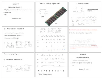
T Flip-Flop (Toggle) CLK State table Q T PS T 0 1 0 0 1 Q’ 1 1 0 Q(t+1) Characteristic Expression Q(t+1) = Q’(t)T(t) + Q(t)T’(t) 7
Using a JK F-F to implement a D and T F-F CLK Q x J Q’ K iClicker The above circuit behaves as which of the following flip flops? A. D F-F B. T F-F C. None of the above 8
Using a JK F-F to implement a D and T F-F CLK Q T J Q’ K T flip flop 9
10
11
12
13
Midterm review True or False 1. In a K-map an implicant can consist of a group of two adjacent cells containing zeros 2. A minterm may evaluate to a one for multiple input combinations. 3. An incompletely specified function results in a minimal circuit whose output cannot be determined for some input combinations. 4. When minimizing a function to product of sum form, we always assume that the don't care terms are 1. 5. The output of combinational circuits depends only on current inputs. 14
Reduce to SOP form F(a,b,c,d)= Π M(3,4,5,6,7,11,12). Π D(10, 15) ab 11 00 01 10 cd 0 4 12 8 00 1 5 13 9 01 3 7 15 11 11 2 6 14 10 10 15
Reduce the following to a SOP form F(a,b,c,d)= Π M(3,4,5,6,7,11,12). Π D(10, 15) ab 11 00 01 10 cd 0 4 12 8 1 0 0 1 00 1 5 13 9 01 1 0 1 1 3 7 15 11 11 0 0 X 0 2 6 14 10 10 1 0 1 X 16
Minimize using Boolean algebra • F(x,y,z)= xy+y’((x+y’)’+z)+xz 17
Design Problem Design a circuit that gives the absolute distance between two 2-bit numbers ( e.g. x=3, y=1, d=2) 18
Design Problem 19
Recommend
More recommend
Explore More Topics
Stay informed with curated content and fresh updates.
