Home Lab 3 Explained Operational Amplifiers (op-amps) Professor - PowerPoint PPT Presentation
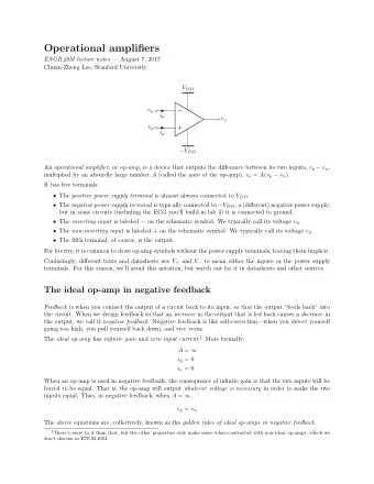
Home Lab 3 Explained Operational Amplifiers (op-amps) Professor Peter YK Cheung Dyson School of Design Engineering URL: www.ee.ic.ac.uk/pcheung/teaching/DE1_EE/ E-mail: p.cheung@imperial.ac.uk PYKC 2 June 2020 Lab 3 Explained Slide 1 DE 1.3
Home Lab 3 Explained Operational Amplifiers (op-amps) Professor Peter YK Cheung Dyson School of Design Engineering URL: www.ee.ic.ac.uk/pcheung/teaching/DE1_EE/ E-mail: p.cheung@imperial.ac.uk PYKC 2 June 2020 Lab 3 Explained Slide 1 DE 1.3 - Electronics 1
Setting things up – 5V power supply PYKC 2 June 2020 Lab 3 Explained Slide 2 DE 1.3 - Electronics 1
Task 1 – Loading effect on SIG_GEN ◆ Measure Vs without 200 ohm load – Vp-p should be around 1.65V ◆ Measure Vs again with 200 ohm load. You will see that Vp-p is reduced due to the internal source resistance of SIG_GEN + = 2.5V DC + 10kHz sine wave Vs 1.65V peak-to-peak 10kHz sine wave - 2.5V DC offset 1.65V peak-to-peak Rs + Vs - 200 PYKC 2 June 2020 Lab 3 Explained Slide 3 DE 1.3 - Electronics 1
Task 2 – Using a Unity Gain Amplifier (1) Topic 11 slide 4 Vs Y = X 10kHz sine wave 1.65V peak-to-peak 200 2.5V DC offset PYKC 2 June 2020 Lab 3 Explained Slide 4 DE 1.3 - Electronics 1
Task 2 – Using a Unity Gain Amplifier (2) ◆ Add R3 (200k) – makes no difference, but ready for Task 3 ◆ Add R1 and R2 to make Pin 3 sitting at 2.5Vdc offset (also ready for later tasks) 200k Pin 1 R1 200k R2 10kHz sine wave 1.65V peak-to-peak 2.5V DC offset Mount resistor on adjacent pins vertically PYKC 2 June 2020 Lab 3 Explained Slide 5 DE 1.3 - Electronics 1
Task 3 – x2 Amplifier Failure (1) ◆ Add R4 – See notes on Topic 11 slide 6. The gain of the amplifier should be x 2. ◆ However, you will see that Vo shows a sine wave with top of it “clipped”. Gain = (1 + R 3 R 4) Topic 11 slide 6 PYKC 2 June 2020 Lab 3 Explained Slide 6 DE 1.3 - Electronics 1
Task 3 – x2 Amplifier Failure (2) ◆ Reason: x2 amplification applies both the 1.65Vp-p sine signal as well as the 2.5V DC offset. So, we will get a 3.3Vp-p sine wave sitting on a 5V offset ◆ Since power supply to op-amp is 5V, no output voltage can exceed this. PYKC 2 June 2020 Lab 3 Explained Slide 7 DE 1.3 - Electronics 1
Task 4 – x2 Amplifier Success (1) ◆ Add C2 and C3, both 1uF. This will now work. Why? + 2.5V DC 10kHz sine wave 1.65V peak-to-peak 2.5V DC offset 10kHz sine wave 1.65V peak-to-peak PYKC 2 June 2020 Lab 3 Explained Slide 8 DE 1.3 - Electronics 1
Task 4 – x2 Amplifier Success (2) ◆ Consider what happens at DC source (principle of superposition): C2 is open-circuit, so 2.5V dc is blocked by C2. Instead, V+ is now at 2.5V 1. because of R1 and R2 (voltage divider). C3 is open-circuit. Therefore the op-amp is now a x1 amplifier as in Task 2. 2. 2.5V 2.5V x1 PYKC 2 June 2020 Lab 3 Explained Slide 9 DE 1.3 - Electronics 1
Task 4 – x2 Amplifier Success (3) ◆ Consider what happens at high frequency (e.g. 10kHz sine wave): C2 is short-circuit, so Vs goes directly to V+. 1. C3 is short-circuit. Therefore the op-amp is now a x2 amplifier as in Task 3.. 2. PYKC 2 June 2020 Lab 3 Explained Slide 10 DE 1.3 - Electronics 1
Task 5 – x101 amplifier failure (1) ◆ Replace R4 with 2k ohm resistor. Gain = 1 + R3/R4 = 101 PYKC 2 June 2020 Lab 3 Explained Slide 11 DE 1.3 - Electronics 1
Task 5 – High gain amplifier failure (2) ◆ Replace R4 with 2k ohm resistor. Gain = 1 + R3/R4 = 101 ◆ Build a 1:101 voltage divider to reduce input signal to amplifier to ~16mV ◆ Change sine wave frequency from 1kHz to 100kHz – see gain of 101 NOT possible beyond 10kHz due to gain-bandwidth product limited to 1MHz. Vcc = 5v 200k R1 0.1 µ 1 µ 8 C1 3 1kHz sine wave + R5 1.65V peak-to-peak Vo 1 2.5V DC offset 100k ½ opamp 200k 1k 2 R2 R6 4 Vs R3 200k 2k R4 1 µ Topic 11 slide 13 PYKC 2 June 2020 Lab 3 Explained Slide 12 DE 1.3 - Electronics 1
Task 6 – High gain amplifier in 2 stages (1) ◆ Stage 1: non-inverting amplifier with GAIN = 11 ◆ Replace R4 with a 20k ohm resistor. Now gain is x11 PYKC 2 June 2020 Lab 3 Explained Slide 13 DE 1.3 - Electronics 1
Task 6 – x101 amplifier in 2 stages (2) ◆ Stage 2: inverting amplifier with GAIN = -10 (circuit in RED) ◆ Now check Vo1 and Vo2 Gain = − R 9 R 10 Topic 11 slide 8 PYKC 2 June 2020 Lab 3 Explained Slide 14 DE 1.3 - Electronics 1
Task 6 – x101 amplifier in 2 stages (3) ◆ Check that Vo1 and Vo2 have opposite phase (i.e. inverting amplifier DOES invert), use PWM signal instead of sine wave signal. PYKC 2 June 2020 Lab 3 Explained Slide 15 DE 1.3 - Electronics 1
Task 7 – Amplifying a real signal ◆ Connect the two amplifier in series (Vo1 becomes input to Vo2) ◆ Add microphone circuit shown. X PYKC 2 June 2020 Lab 3 Explained Slide 16 DE 1.3 - Electronics 1
Task 8 – Audio Amplifier for 8 ohm speaker (optional) ◆ Op-amp only can only deliver at most 20mA current at its output ◆ Need special amplifier to drive 8 ohm speaker ◆ Use special amplifier for this purpose PYKC 2 June 2020 Lab 3 Explained Slide 17 DE 1.3 - Electronics 1
Recommend
More recommend
Explore More Topics
Stay informed with curated content and fresh updates.
