flux fluoresces under uv light
play

flux fluoresces under UV light This paper reviews the test methods - PDF document

Originally published in the Proceedings of IPC APEX/EXPO, March 2014 Development, Testing and Implementation of SAMP-Based Stencil Nano Coatings Chrys Shea Shea Engineering Services Burlington, NJ, USA Ray Whittier Vicor VI CHiP Division


  1. Originally published in the Proceedings of IPC APEX/EXPO, March 2014 Development, Testing and Implementation of SAMP-Based Stencil Nano Coatings Chrys Shea Shea Engineering Services Burlington, NJ, USA Ray Whittier Vicor VI CHiP Division Andover, MA, USA Eric Hanson Aculon San Diego, CA, USA Abstract Stencil nanocoatings have demonstrated significant improvements in numerous aspects of solder paste printing, including print yield, transfer efficiency, print definition and under wipe requirements. By lowering the surface energy of SMT stencils, they reduce flux bleed out around the perimeters of apertures and enable cleaner paste release during stencil-PCB separation. With several years of commercial success behind the original nanocoating materials, a new generation has been developed that improves upon many of the characteristics of the original formulations. Advancements in durability, detectability and cost boost the overall performance of these flux-repellent stencil treatments. Numerous tests have been performed to characterize stencil nanocoating materials throughout their development cycles and quantify their actual performance in SMT production environments. Laboratory tests have used liquid contact 
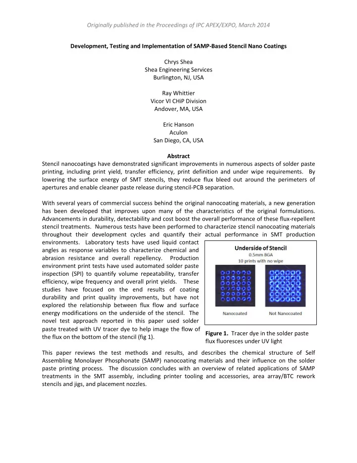
angles as response variables to characterize chemical and abrasion resistance and overall repellency. Production environment print tests have used automated solder paste inspection (SPI) to quantify volume repeatability, transfer efficiency, wipe frequency and overall print yields. These studies have focused on the end results of coating durability and print quality improvements, but have not explored the relationship between flux flow and surface energy modifications on the underside of the stencil. The novel test approach reported in this paper used solder paste treated with UV tracer dye to help image the flow of Figure 1. Tracer dye in the solder paste the flux on the bottom of the stencil (fig 1). flux fluoresces under UV light This paper reviews the test methods and results, and describes the chemical structure of Self Assembling Monolayer Phosphonate (SAMP) nanocoating materials and their influence on the solder paste printing process. The discussion concludes with an overview of related applications of SAMP treatments in the SMT assembly, including printer tooling and accessories, area array/BTC rework stencils and jigs, and placement nozzles.

  2. Originally published in the Proceedings of IPC APEX/EXPO, March 2014 Introduction to Solder Paste Print Analysis Nanocoatings are referred to as hydrophobic – repelling water, oleophobic – repelling oil, and fluxophobic – repelling solder paste flux. Their theory of operation is based on reducing the adhesion of solder paste to the SMT stencil. The adhesive properties of solder paste play a large role in print quality. Paste sticks to both the stencil and the PCB, and during the separation phase of the print process, the forces holding the paste to the PCB compete with the forces holding the paste in the stencil. The competing forces are proportional to the contact areas of both surfaces. The relationship between the contact areas is mathematically modeled by a quotient known as the Area Ratio (AR). Figure 2. Area Ratio and Transfer Efficiency information Figure 3. Diagram of solder paste transfer process The AR is typically calculated as the area of the aperture on the circuit side divided by the area of the aperture walls as seen in figure 2. 1 Variations on the AR calculation are sometimes incorporated,

  3. Originally published in the Proceedings of IPC APEX/EXPO, March 2014 including substituting actual pad area for aperture area, simplifying calculations for squares with rounded corners by using formulas for simple squares, or calculating wall areas based on straight vs. trapezoidal geometries. Regardless of the details in the calculations, all the formulas attempt to model the AR because it helps predict the proportion of solder paste that gets transferred to the PCB, referred to as the Transfer Efficiency (TE). At certain AR thresholds, the opposing adhesive forces tear the thixotropic solder paste material, depositing some on the PCB and leaving some behind in the aperture, as shown in figure 3. 1 The AR-TE relationship varies from paste to paste and process to process, but typically, ARs greater than 0.80 produce nearly 100% TE, and ARs between .65 and 0.80 produce 75- 100% TE. ARs less than 0.65 are not recommended with general SMT processes and materials because they result in insufficient and highly variable TE, significantly reducing print and assembly yields. TE is a commonly employed metric in stencil printing to quantify the performance of stencils, pastes or print parameters. As important as TE – and arguably more so - is volume repeatability. Fine feature SMT devices require consistent prints. A large format BGA can have over 2000 I/O on one device. One insufficient or excessive paste deposit can cause a failure that requires all of the device’s joints to be desoldered and resoldered in the rework process, jeopardizing the functionality and reliability of the entire assembly. Print volume repeatability is typically calculated based on measurements of a specific feature size. The standard deviation of the paste volume readings are divided by the average of the volume readings. It is known as the Coefficient of Variation (CV) in statistical terms, and is usually expressed as a percentage in the context of print volume repeatability, with lower values being better than higher ones. CVs of 10% or less generally indicate acceptable print repeatability. As ARs get smaller, CVs usually get larger. Deposit volumes are typically measured with laser- or white light-based automated Solder Paste Inspection (SPI) systems. A third and less quantifiable factor in print quality is print definition. Whereas TE and CV are based on numerical measurements, print definition is based on a Likert scale that uses visual assessment. An ideal solder paste print will have a prismatic form - typically round, square or rectangular when viewed from the top down - with vertical sides and a flat top. As AR begins to decrease, the verticality of the sides diminishes and the top becomes rounded. The loss of crisp print definition is a direct result of the tearing of the solder paste upon release from the stencil. It is manifested as continued loss of prismatic form in the deposits as AR continues to decrease, and other geometric aberrations such as tall peaks on the deposits or strings of solder paste that fall over on the PCB to bridge multiple deposits often occur. Print definition is usually judged on a scale of 1-5, with 1 being unacceptable and 5 representing the ideal form. Appendix A shows an example of visual standards for rating print definition. Background Initial testing of nanocoating in 2011 2 revealed vastly improved print quality when nanocoating was applied to SMT stencils. Tested on 13 pairs of stencils manufactured by electroforming, laser cutting, or both, the coating dramatically improved the yields of nearly every pair, as seen in figure 4. Based on the test results, the nanocoating was applied to all the high volume stencils in the PCB assembly operation, and overall print yields increased by approximately 5%.

  4. Originally published in the Proceedings of IPC APEX/EXPO, March 2014 Figure 4. Effects of nanocoating on print yields for a variety of stencil types in initial (2011) study 2 Figure 5a : Effects of stencil materials on overall Figure 5b : Effects of stencil materials on µBGA print yields transfer efficiencies Figure 5c: Effects of stencil materials on print volume repeatabilities Figure 5. Print test results from subsequent (2013) study 3

  5. Originally published in the Proceedings of IPC APEX/EXPO, March 2014 A subsequent set of formal experiments on the nanocoatings in 2013 3 compared the new generation of material to the 1 st generation. Stencils with the new generation of nanocoating (Nano2) consistently produced higher print yields and lower CVs than stencils treated with the original nanocoating (Nano1) and untreated stencils. Stencils coated with Nano2 also produced slightly lower TEs than untreated stencils, which, as explored in these tests, may be due to improved print definition. Figures 5a through 5c summarize the test results. The µBGA prints reported in the results were based on 10.5mil circular apertures in a 4mil FG foil, with an AR of 0.66. Fig. 6a. Effect of stencil under wipe on print yield Fig. 6b Effect of stencil under wipe on transfer efficiency Fig. 6c . Effect of stencil under wipe on print volume variation Figure 6. Stencil under wipe frequency print test results 3 The 2013 experiments also tested wipe frequency. The production process used a vacuum/dry/vacuum wipe after every print. The two conditions tested were the production process at 1 print per wipe, and an extended process of 10 prints before the wipe. The results are shown in figures 6a through 6b. The process with 10 prints and no wipe produced higher yields and lower CVs than the process with 1 print per wipe for both nanocoatings. In both cases the newer nanocoating performed better than the original. The consistently higher yields and lower volume variations found in the latter set of experiments was anticipated and expected, based on the original experiments and production history. The increase in

Download Presentation
Download Policy: The content available on the website is offered to you 'AS IS' for your personal information and use only. It cannot be commercialized, licensed, or distributed on other websites without prior consent from the author. To download a presentation, simply click this link. If you encounter any difficulties during the download process, it's possible that the publisher has removed the file from their server.

Recommend


More recommend