
SLIDE 1
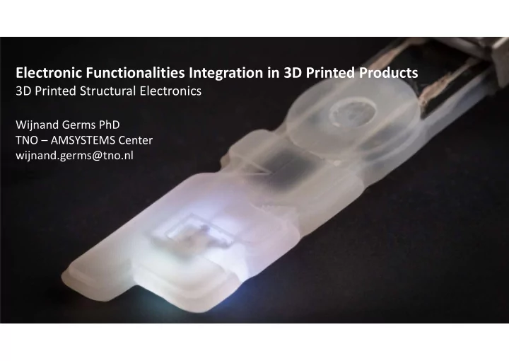
Electronic Functionalities Integration in 3D Printed Products
3D Printed Structural Electronics
Wijnand Germs PhD TNO – AMSYSTEMS Center wijnand.germs@tno.nl
Electronic Functionalities Integration in 3D Printed Products 3D - - PowerPoint PPT Presentation
Electronic Functionalities Integration in 3D Printed Products 3D Printed Structural Electronics Wijnand Germs PhD TNO AMSYSTEMS Center wijnand.germs@tno.nl Alliance between TNO and TU/e-HTSC to accelerate the development of the next
3D Printed Structural Electronics
Wijnand Germs PhD TNO – AMSYSTEMS Center wijnand.germs@tno.nl
Alliance between TNO and TU/e-HTSC to accelerate the development of the next generation equipment for industrial additive manufacturing 3D Printed Structural Electronics, a joint activity of two TNO Centers: Holst Center – Printed Electronics AMSYSTEMS Center – equipment for industrial additive manufacturing
Highly optimized manufacturing processes Assembly of housings and PCBs Drawbacks of conventional manufacturing High investement levels for equipment and tooling → small series / product diversity unatractive Strandardized product designs → Limited shape freedom Rigid and fragmented supply chain → increasing lead times, decreasing flexibility Conventional manufacturing – tool centricity 3D Printed Electronics – data centricity
→ Minimized $$
3D Printing Printed Electronics
Electronic functionality integration in products
Sensors, lighting, actuators, including data processing Reduced number of parts - reduced volume
Personalization/Customization
Ear buds, hearing aids, customized consumer products Low cost for low series – No product specific tooling
Shorter lead times
Agile manufacturing – No product specific tooling
3D PRINTED STRUCTURAL ELECTRONICS USING SLA AND SLS StereoLithography Apparatus (SLA)
Liquid photopolymer Local solidification by UV
Selective Laser Sintering (SLS)
Polymer powder Local sintering by laser
WHY SLA FOR STRUCTURAL ELECTRONICS
Smart Connectors Metamaterial antenna arrays Waveguides Lighting Microfluidics
WHY SLS FOR STRUCTURAL ELECTRONICS
Smart Knee Ankle Foot Orthosis Automotive Orthosis
Published as: Maalderink et al.,Plastics, Rubber and Composites; 2018; Vol 47, No 1, 35-41. Innovation Award at PMI 2016
International Conference
Innovations
Movie on: http://amsystemscenter.com/how-3d-printing-is-combined-with-printed-electronics-technologies/
Two examples: Personalization at unit level No product specific tooling Incorporated micro-systems No PCB required Inherently encapsulated: dust/dirt proof Reducing size Free form
Gear shifter knob - Electronics in small volume
Personalized USB flash drive
Products Industrialization Processes, materials & equipment knowhow materials processes equipment integrated systems new products The Hyb-Man project will develop hybrid 3D manufacturing methods to enable flexible first time right production of smart systems
7
Evaluation SLA material NextDent C&B
Non-reversible degradation starting at 250°C
→ HDT To be done
At -40°C Complex modulus 1,6 GPa At 150°C Complex modulus 0,014 GPa
Youngs modulus 3,5 GPa Tensile strength max 72 MPa Tensile strength break 66 MPa
Henkel WIK20489 ink on SLA substrate
Personalized USB drive
Prediction of internal stresses and warpage Prediction of temperature field Suitable for multiple AM techniques and materials Gcode geometry input
13
Realtime detection of small movement
Autonomous driving
Free 3D oriented metallic features Invisible - Intergated in car parts (bumper)
Gesture Control
Good agreement between simulation and measurement
Innovation award 39th ESA Antenna Workshop 2018
Conference Paper by Yepes et al. Together with TNO Defense, Safety and Security and TU Delft
Movement Assisting Devices: Manufacturing of personalized Kineto- Dynamics parts and products for workers, elderly and children Selective laser sintering
This project has received funding from the European Union’s Horizon 2020 research and innovation programme under grant agreement No 680754
Smart Knee Ankle Foot Orthosis Sit to stand orthosis
Electronic products can be designed and manufactured, with the electronic functions and the functional product shape being fully integrated, to serve the users’ need. Improved product Optimal functionality. The electronics and the mechanical design are optimal, and do not have to do concessions to each other. Cost reduction Small series production is not hindered by high investment in product specific tooling Product development process For the design process there will be a seamless connection between the mechanical design suite and the electronic design suite The resulting CAD file includes everything, and can be sent to the manufacturing line/machine. The manufacturing line/machine is a multi-technology platform and can determine itself which project step is performed in which phase of the production process.
Design software !
3D electronics design Seamless connection between electronic design and mechanical design Design rules depending on technologies used
Process needs to be developed !
Different 3DP technologies exist Different printed electronics technologies exist. Deposition, curing, p&p.
Equipment needs to be developed !
Open platform to do multitechnology/hybrid 3D manufacturing
Materials need to be improved
Fire retardant, temperature resistance, biocompatible, strength, heat conductivity
Certification and standardization
What is suitable for which application, e.g. fire retardant vs. biocompatible
Product life cycle, recyclability
AMSYSTEMS/HOLST
OUTLOOK
Metamaterial antenna arrays Lighting Printed electronics on SLS products
Team members at EU projects: Key partners: AMSYSTEMS: Fabien Bruning Hessel Maalderink John van der Werff Edwin van den Eijnden Mathijs de Schipper Henk Buining Jeroen Smeltink Jeroen Knippeberg Joris Remmers Joris Dufils Frits Verhoeven
This project has received funding from the European Union’s Horizon 2020 research and innovation programme under grant agreement No 680754
Innovation Center by TNO and TU/e HTSC
Explore more on amsystems.com wijnand.germs@tno.nl