device i o
play

Device I/O Configurability isnt free Bake-in some reasonable - PDF document

11/14/11 Overview Many artifacts of hardware evolution Device I/O Configurability isnt free Bake-in some reasonable assumptions Programming Initially reasonable assumptions get stale Find ways to work-around


  1. 11/14/11 ¡ Overview ò Many artifacts of hardware evolution Device I/O ò Configurability isn’t free ò Bake-in some reasonable assumptions Programming ò Initially reasonable assumptions get stale ò Find ways to work-around going forward ò Keep backwards compatibility Don Porter CSE 506 ò General issues and abstractions 
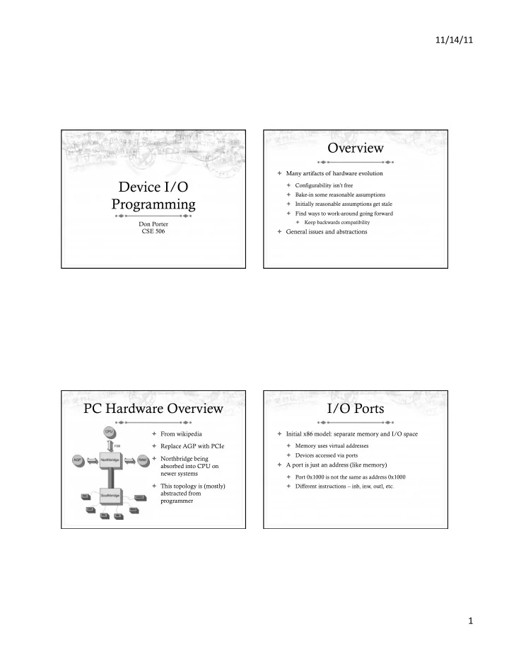
PC Hardware Overview I/O Ports ò From wikipedia ò Initial x86 model: separate memory and I/O space ò Replace AGP with PCIe ò Memory uses virtual addresses ò Devices accessed via ports ò Northbridge being ò A port is just an address (like memory) absorbed into CPU on newer systems ò Port 0x1000 is not the same as address 0x1000 ò This topology is (mostly) ò Different instructions – inb, inw, outl, etc. abstracted from programmer 1 ¡

  2. 11/14/11 ¡ Parallel port (+I/O ports) More on ports (from Linux Device Drivers) ò A port maps onto input pins/registers on a device 7 6 5 4 3 2 1 0 17 16 14 1 Control port: base_addr + 2 ò Unlike memory, writing to a port has side-effects irq enable 7 6 5 4 3 2 1 0 Status port: base_addr + 1 11 10 12 13 15 ò “Launch” opcode to /dev/missiles ò So can reading! 7 6 5 4 3 2 1 0 9 8 7 6 5 4 3 2 Data port: base_addr + 0 ò Memory can safely duplicate operations/cache results 1 14 ò Idiosyncrasy: composition doesn’t necessarily work KEY ò outw 0x1010 <port> != outb 0x10 <port> Input line Output line 3 2 Bit # outb 0x10 <port+1> 17 16 Pin # noninverted inverted 25 13 Figure 9-1. The pinout of the parallel port Port permissions Buses ò Buses are the computer’s “plumbing” between major ò Can be set with IOPL flag in EFLAGS components ò Or at finer granularity with a bitmap in task state ò There is a bus between RAM and CPUs segment ò There is often another bus between certain types of ò Recall: this is the “other” reason people care about the devices TSS ò For inter-operability, these buses tend to have standard specifications (e.g., PCI, ISA, AGP) ò Any device that meets bus specification should work on a motherboard that supports the bus 2 ¡

  3. 11/14/11 ¡ Clocks Clock imbalance (again, but different) ò CPU Clock Speed: What does it mean at electrical level? ò All processors have a clock ò New inputs raise current on some wires, lower on others ò Including the chips on every device in your system ò How long to propagate through all logic gates? ò Network card, disk controller, usb controler, etc. ò Clock speed sets a safe upper bound ò And bus controllers have a clock ò Things like distance, wire size can affect propagation time ò Think now about older devices on a newer CPU ò At end of a clock cycle read outputs reliably ò Newer CPU has a much faster clock cycle ò May be in a transient state mid-cycle ò Not talking about timer device, which raises interrupts at ò It takes the older device longer to reliably read input from wall clock time; talking about CPU GHz a bus than it does for the CPU to write it More clock imbalance CISC silliness? ò Ex: a CPU might be able to write 4 different values into a ò Is there any good reason to use dedicated instructions device input register before the device has finished one clock and address space for devices? cycle ò Why not treat device input and output registers as ò Driver writer needs to know this regions of physical memory? ò Read from manuals ò Driver must calibrate device access frequency to device speed ò Figure out both speeds, do math, add delays between ops ò You will do this in lab 6! (outb 0x80 is handy!) 3 ¡

  4. 11/14/11 ¡ Simplification Optimizations ò Map devices onto regions of physical memory ò How does the compiler (and CPU) know which regions have side-effects and other constraints? ò Hardware basically redirects these accesses away from RAM at same location (if any), to devices ò It doesn’t: programmer must specify! ò A bummer if you “lose” some RAM ò Win: Cast interface regions to a structure ò Write updates to different areas using high-level languages ò Still subject to timing, side-effect caveats Optimizations (2) volatile keyword ò Recall: Common optimizations (compiler and CPU) ò A volatile variable cannot be cached in a register ò Out-of-order execution ò Writes must go directly to memory ò Reorder writes ò Reads must always come from memory/cache ò Cache values in registers ò volatile code blocks cannot be reordered by the compiler ò When we write to a device, we want the write to really ò Must be executed precisely at this point in program happen, now! ò E.g., inline assembly ò Do not keep it in a register, do not collect $200 ò __volatile__ means I really mean it! ò Note: both CPU and compiler optimizations must be disabled 4 ¡

  5. 11/14/11 ¡ Compiler barriers CPU Barriers ò Inline assembly has a set of clobber registers ò Advanced topic: Don’t need details ò Basic idea: In some cases, CPU can issue loads and ò Hand-written assembly will clobber them stores out of program order (optimize perf) ò Compiler’s job is to save values back to memory before inline asm; no caching anything in these registers ò Subject to many constraints on x86 in practice ò “memory” says to flush all registers ò In some cases, a “fence” instruction is required to ensure that pending loads/stores happen before the CPU moves ò Ensures that compiler generates code for all writes to forward memory before a given operation ò Rarely needed except in device drivers and lock-free data structures Configuration ISA memory hole ò Where does all of this come from? ò Recall the “memory hole” from lab 2? ò Who sets up port mapping and I/O memory mappings? ò 640 KB – 1 MB ò Who maps device interrupts onto IRQ lines? ò Required by the old ISA bus standard for I/O mappings ò Generally, the BIOS ò No one in the 80s could fathom > 640 KB of RAM ò Sometimes constrained by device limitations ò Devices sometimes hard-coded assumptions that they would be in this range ò Older devices hard-coded IRQs ò Generally reserved on x86 systems (like JOS) ò Older devices may only have a 16-bit chip ò Strong incentive to save these addresses when possible ò Can only access lower memory addresses 5 ¡

  6. 11/14/11 ¡ New hotness: PCI More flexibility ò Hard-coding things is bad ò PCI addressing (both memory and I/O ports) are dynamically configured ò Willing to pay for flexibility in mapping devices to IRQs ò Generally by the BIOS and memory regions ò But could be remapped by the kernel ò Guessing what device you have is bad ò Configuration space ò On some devices, you had to do something to create an ò 256 bytes per device (4k per device in PCIe) interrupt, and see what fired on the CPU to figure out what IRQ you had ò Standard layout per device, including unique ID ò Need a standard interface to query configurations ò Big win: standard way to figure out my hardware, what to load, etc. PCI Configuration Layout PCI Overview From device driver book ò Most desktop systems have 2+ PCI buses 0x0 0x1 0x2 0x3 0x4 0x5 0x6 0x7 0x8 0x9 0xa 0xb 0xc 0xd 0xe 0xf Revis- Vendor Device Command Status Class Code Cache Latency Header BIST 0x00 ion ID ID Reg. Reg. Line Timer Type ò Joined by a bridge device ID Base Base Base Base ò Forms a tree structure (bridges have children) 0x10 Address 0 Address 1 Address 2 Address 3 Base Base CardBus Subsytem Subsytem 0x20 Device ID Address 4 Address 5 CIS pointer Vendor ID Min_Gnt Max_Lat Expansion ROM IRQ IRQ Reserved 0x30 Base Address Line Pin - Required Register - Optional Register Figure 12-2. The standardized PCI configuration registers 6 ¡

  7. 11/14/11 ¡ PCI Layout PCI Addressing From Linux Device Drivers ò Each peripheral listed by: PCI Bus 0 PCI Bus 1 Host Bridge PCI Bridge ò Bus Number (up to 256 per domain or host) RAM CPU ò A large system can have multiple domains ò Device Number (32 per bus) ISA Bridge ò Function Number (8 per device) ò Function, as in type of device, not a subroutine ò E.g., Video capture card may have one audio function and CardBus Bridge one video function ò Devices addressed by a 16 bit number Figure 12-1. Layout of a typical PCI system Direct Memory Access PCI Interrupts (DMA) ò Each PCI slot has 4 interrupt pins ò Simple memory read/write model bounces all I/O through the CPU ò Device does not worry about how those are mapped to IRQ lines on the CPU ò Fine for small data, totally awful for huge data ò Idea: just write where you want data to go (or come ò An APIC or other intermediate chip does this mapping from) to device ò Bonus: flexibility! ò Let device do bulk data transfers into memory without ò Sharing limited IRQ lines is a hassle. Why? CPU intervention ò Trap handler must demultiplex interrupts ò Interrupt CPU on I/O completion (asynchronous) ò Being able to “load balance” the IRQs is useful 7 ¡

Download Presentation
Download Policy: The content available on the website is offered to you 'AS IS' for your personal information and use only. It cannot be commercialized, licensed, or distributed on other websites without prior consent from the author. To download a presentation, simply click this link. If you encounter any difficulties during the download process, it's possible that the publisher has removed the file from their server.

Recommend


More recommend