Constructing a Crystal Once you specify the lattice, you can then - - PowerPoint PPT Presentation

constructing a crystal
SMART_READER_LITE
LIVE PREVIEW

Constructing a Crystal Once you specify the lattice, you can then - - PowerPoint PPT Presentation

Constructing a Crystal Once you specify the lattice, you can then hang a collection of atoms off of each position in the lattice Important: every lattice point (point on the scaffold) must have the exact same environment.


slide-1
SLIDE 1

EE-452 13 - 1

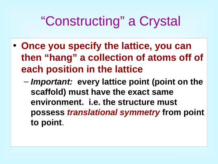
“Constructing” a Crystal

  • Once you specify the lattice, you can

then “hang” a collection of atoms off of each position in the lattice

– Important: every lattice point (point on the scaffold) must have the exact same

  • environment. i.e. the structure must

possess translational symmetry from point to point.

slide-2
SLIDE 2

EE-452 13 - 2

Crystal Bravais Lattices

  • Simple Base

Centered Triclinic Monoclinic Orthorhombic

Simple Body centered Base centered Face Centered

Hexagonal

slide-3
SLIDE 3

EE-452 13 - 3

Crystal lattices ( cont.)

Rhombohedral Tetragonal Simple Body Centered

slide-4
SLIDE 4

EE-452 13 - 4

Simple Cubic lattices

Simple Body-Centered Face-centered

slide-5
SLIDE 5

EE-452 13 - 5

Atomic Order of a Crystal Structure

Figure 4.2

Plummer

slide-6
SLIDE 6

EE-452 13 - 6

Amorphous Atomic Structure

Figure 4.3

Plummer

slide-7
SLIDE 7

EE-452 13 - 7

4

  • Rare due to poor packing (only Po has this structure)
  • Close-packed directions are cube edges.
  • Coordination # = 6

(# nearest neighbors)

SIMPLE CUBIC STRUCTURE (SC)

back

slide-8
SLIDE 8

EE-452 13 - 8

Unit Cell in 3-D Structure

Unit cell

Figure 4.4

Plummer

slide-9
SLIDE 9

EE-452 13 - 9

10

  • Coordination # = 12
  • ABAB... Stacking Sequence
  • APF = 0.74
  • 3D Projection
  • 2D Projection

A sites B sites A sites Bottom layer Middle layer Top layer

Adapted from Fig. 3.3, Callister 6e.

Hexagonal Close-Packed Structure (hcp)

Note: this structure is NOT cubic back

slide-10
SLIDE 10

EE-452 13 - 10

Body-Centered Cubic (BCC)

slide-11
SLIDE 11

EE-452 13 - 11

Specifying Directions in Crystals

slide-12
SLIDE 12

EE-452 13 - 12

Silicon Crystal Structure and Growth (Plummer - Chapter 3)

Click to edit Master text styles Second level

  • Third level
  • Fourth level
  • Fifth level

Plummer

slide-13
SLIDE 13

EE-452 13 - 13

Miller Indices of Crystal Planes

Z X Y (100) Z X Y (110) Z X Y (111)

Figure 4.9

lummer

slide-14
SLIDE 14

EE-452 13 - 14

Silicon Crystal Structure

  • Planes and directions are defined using x, y, z coordinates.
  • [111] direction is defined by a vector of 1 unit in x, y and z.
  • Planes defined by “Miller indices” – Their normal direction (reciprocals of intercepts of

plane with the x, y and z axes).

Crystals are characterized by a unit cell which repeats in the x, y, z directions.

Plummer

slide-15
SLIDE 15

EE-452 13 - 15

Silicon has the basic diamond crystal structure – two merged FCC cells offset by a/4 in x, y and z.

Plummer

slide-16
SLIDE 16

EE-452 13 - 16

Various types of defects can exist in a crystal (or can be created by processing steps). In general, these cause electrical leakage and are result in poorer devices.

(Extra line of atoms)

slide-17
SLIDE 17

EE-452 13 - 17

Point Defects

Vacancy defect Interstitial defect Frenkel defect

slide-18
SLIDE 18

EE-452 13 - 18