
SLIDE 1
Implementation+Technologies
- We+can+implement a+design+with+many+different+
implementation+technologies+8 different+ implementation+technologies+offer+different+ tradeoffs
– HDL+Synthesis offers+an+easy+way+to+target+a+model+ toward+different+implementations – There+are+also+re8targeting+tools+which+will+convert+a+ netlist+from+one+technology+to+another+(from+a+standard+ cell+implementation+to+a+Field+Programmable+Gate+ Array+implementation).
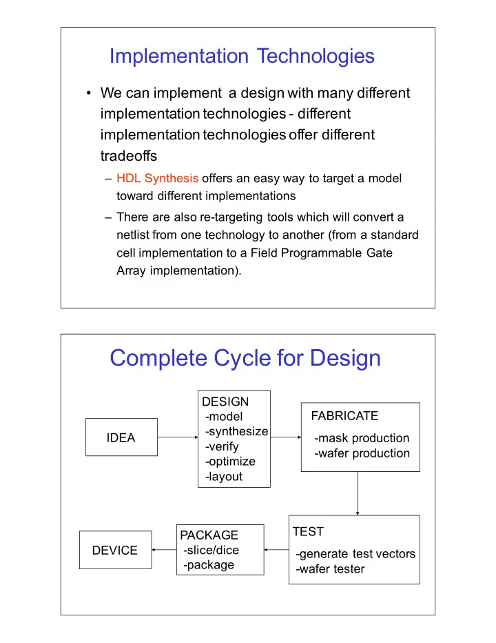
Complete+Cycle+for+Design
IDEA DESIGN 8model 8synthesize 8verify 8optimize 8layout PACKAGE 8slice/dice 8package FABRICATE 8mask+production+++ 8wafer+production TEST 8generate+test+vectors 8wafer+tester DEVICE