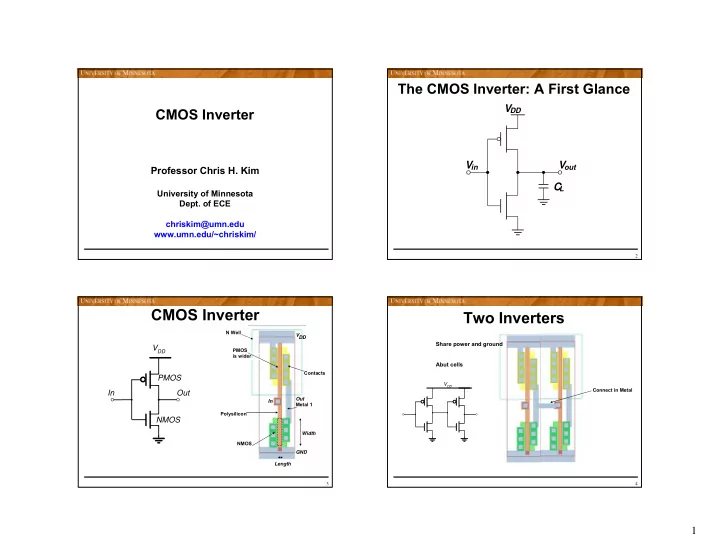
cmos inverter two inverters
play

CMOS Inverter Two Inverters N Well VDD Share power and ground V - PowerPoint PPT Presentation

The CMOS Inverter: A First Glance V CMOS Inverter DD V in V out Professor Chris H. Kim C L University of Minnesota Dept. of ECE chriskim@umn.edu www.umn.edu/~chriskim/ 2 CMOS Inverter Two Inverters N Well VDD Share power and ground V


  1. The CMOS Inverter: A First Glance V CMOS Inverter DD V in V out Professor Chris H. Kim C L University of Minnesota Dept. of ECE chriskim@umn.edu www.umn.edu/~chriskim/ 2 CMOS Inverter Two Inverters N Well VDD Share power and ground V DD PMOS is wider Abut cells Contacts PMOS V DD Connect in Metal In Out Out In Metal 1 Polysilicon NMOS Width NMOS GND Length 3 4 1

  2. CMOS Inverter First-Order DC Analysis V DD V DD Voltage Transfer R p V OL = 0 Characteristics V OH = V DD V M = f(R n , R p ) V out V out R n V in = V DD V in = 0 6 CMOS Inverter VTC CMOS Inverter Load Characteristics NMOS off PMOS lin 2.5 I Dn NMOS sat V in = 0 V in = 2.5 PMOS lin 2 PMOS in = 0.5 V in = 2 NMOS V V out NMOS sat 1.5 PMOS sat in = 1 in = 1.5 V V 1 NMOS lin in = 1.5 V in = 1 V PMOS sat 0.5 NMOS lin in = 1.5 V in = 1 V V in = 2 PMOS off in = 0.5 V in = 2.5 V in = 0 V 0.5 1 1.5 2 2.5 V in V out 7 8 2

  3. Simulated Inverter VTC (hspice) Switching Threshold as a Function of Transistor Ratio 2.5 1.8 2 1.7 1.6 1.5 V out (V) 1.5 V (V) 1.4 M 1.3 1 1.2 1.1 0.5 1 0.9 0 0 0.5 1 1.5 2 2.5 0.8 10 0 10 1 V in (V) W p /W n 9 10 VTC as a function of VDD Impact of Sizing 2.5 2.5 0.2 2 Wider 2 PMOS 0.15 1.5 out (V) 1.5 out (V) Symmetrical out (V) 0.1 Wider V V V 1 1 NMOS 0.05 0.5 0.5 Gain=-1 0 0 0 0.05 0.1 0.15 0.2 0 0.5 1 1.5 2 2.5 V in (V) 0 V in (V) 0 0.5 1 1.5 2 2.5 V in (V) 11 12 3

  4. Impact of Process Variations DC Operation Voltage Transfer Characteristic 2.5 V(y) VOH = f (VOL) 2 Fast PMOS VOH f VOL = f (VOH) Slow NMOS V(y)=V(x) VM = f (VM) out (V) 1.5 Nominal Switching Threshold Fast NMOS V V M 1 Slow PMOS VOL 0.5 VOL VOH V(x) 0 0 0.5 1 1.5 2 2.5 V in (V) Nominal Voltage Levels 13 14 Mapping between analog and digital Definition of Noise Margins signals Vout "1" VOH “ 1” Slope = -1 V OH VOH VIH NM H Noise margin high VIH Undefined Undefined Region Region VIL NM L Noise margin low VOL Slope = -1 VIL "0" V OL Gate Input “ 0” VOL Gate Output VIL VIH Vin 15 16 4

  5. Regenerative Property Example: CMOS Inverter DC Properties out out v 3 v 3 • V OH = V DD = 2.5V f (v) fin v(v) • V OL = 0V v 1 v 1 • V IL = 1.05V v 3 fin v(v) f (v) • V IH = 1.45V • N MH =1.05V • N ML = 1.05V v 2 v 0 in v 0 v 2 in • V M = 1.2V Regenerative Non-Regenerative 17 18 Regenerative Property v0 v1 v2 v v v v 3 4 5 6 A chain of inverters Propagation Delay 5 v 0 V (Volt) 3 v 1 1 v 2 2 1 0 2 4 6 8 10 Simulated response t (nsec) 19 5

  6. Computing the Capacitances CMOS Inverter: Transient Response V DD V DD V DD V DD t pHL = f(R on .C L ) M 2 R p M 4 C g 4 C db 2 = 0.69 R on C L C gd 12 V out V out 2 V in V out C db 1 C w C g 3 V out M 3 M 1 C L Interconnect C L R n Fanout V in V out Simplified C L Model V in = 0 V in = V DD (a) Low-to-high (b) High-to-low 21 22 Delay Definitions CMOS Inverter Propagation Delay V in V DD 50% t pHL = C L V dd /2 I av t t pHL t pLH V out V out 90% I av C L 50% t 10% t f t r V in = V DD 23 24 6

  7. Design for Performance Transient Response • Keep capacitances small 3 • Increase transistor sizes 2.5 2 – watch out for self-loading! t p = 0.69 C L (R eqn +R eqp )/2 • Increase V DD 1.5 out (V) t pHL t pLH V 1 0.5 0 -0.5 0 0.5 1 1.5 2 2.5 t (sec) -10 x 10 25 26 Device Sizing Delay as a function of V DD -11 3.8 x 10 5.5 (for fixed load) 5 3.6 t p (normalized) 4.5 3.4 4 3.2 t p (sec) 3.5 3 3 2.8 Self-loading effect: Intrinsic capacitances 2.5 2.6 dominate 2 2.4 1.5 2.2 1 2 0.8 1 1.2 1.4 1.6 1.8 2 2.2 2.4 2 4 6 8 10 12 14 Size Vdd (V) 27 28 7

  8. NMOS/PMOS ratio Impact of Rise Time on Delay -11 5x 10 0.35 tpHL tpLH 4.5 0.3 t pHL (nsec) tp t p (sec) 0.25 β = W p /W n 4 0.2 3.5 0.15 0 0.2 0.4 0.6 0.8 1 t rise (nsec) 3 1 1.5 2 2.5 3 3.5 4 4.5 5 β t p = t step ( i ) + ht step ( i -1) 29 30 Ring Oscillator Fan-in and Fan-out v 0 v 1 v 2 v 3 v 4 v 5 M N v 0 v 1 v 5 Fan-out N Fan-in M T = 2 × t p × N 31 32 8

  9. CMOS Properties • Full rail-to-rail swing • Symmetrical VTC • Propagation delay function of load capacitance and resistance of transistors • No static power dissipation (ignoring leakage current) • Direct path current during switching 33 9

Download Presentation
Download Policy: The content available on the website is offered to you 'AS IS' for your personal information and use only. It cannot be commercialized, licensed, or distributed on other websites without prior consent from the author. To download a presentation, simply click this link. If you encounter any difficulties during the download process, it's possible that the publisher has removed the file from their server.

Recommend


More recommend