
SLIDE 1
1
CMOS Inverter: Power Dissipation and Sizing
Professor Chris H. Kim
University of Minnesota
- Dept. of ECE
chriskim@umn.edu
CMOS Inverter Power Dissipation
3
Where Does Power Go in CMOS?
- Switching power
– Charging capacitors
- Leakage power
– Transistors are imperfect switches
- Short-circuit power
– Both pull-up and pull-down on during transition
- Static currents
– Biasing currents, in e.g. memory
4
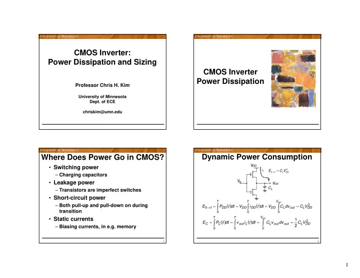
Dynamic Power Consumption
( ) ( )
∫ ∫ ∫
= = = =
→
DD
V DD L
- ut
L DD T T DD DD DD
V C dv C V dt t i V dt t P E
2 1
( ) ( )
∫ ∫ ∫
= = = =
DD
V DD L
- ut
- ut
L T T L
- ut
C C
V C dv v C dt t i v dt t P E
2
2 1
iL
2 1 DD LV
C E =
→
V
in
V
- ut
CL V
DD