
SLIDE 1
02/05/2014 1
Slide 2-32
Chapter 2 Motion and Recombination
- f Electrons and Holes
2.1 Thermal Motion
Average electron or hole kinetic energy
2
2 1 2 3
th
mv kT
kg 10 1 . 9 26 . K 300 JK 10 38 . 1 3 3
31 1 23
eff th
m kT v cm/s 10 3 . 2 m/s 10 3 . 2
7 5
Slide 1-32 Slide 2-33
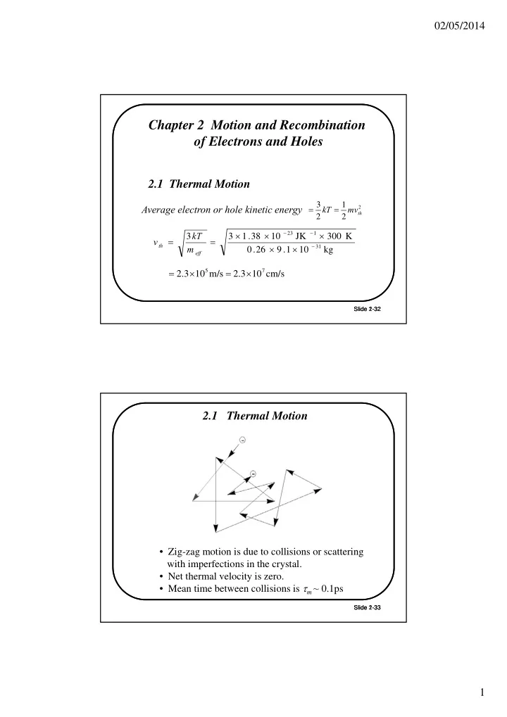
2.1 Thermal Motion
- Zig-zag motion is due to collisions or scattering
with imperfections in the crystal.
- Net thermal velocity is zero.
- Mean time between collisions is m ~ 0.1ps
Slide 1-33