
SLIDE 1
02/05/2014 1
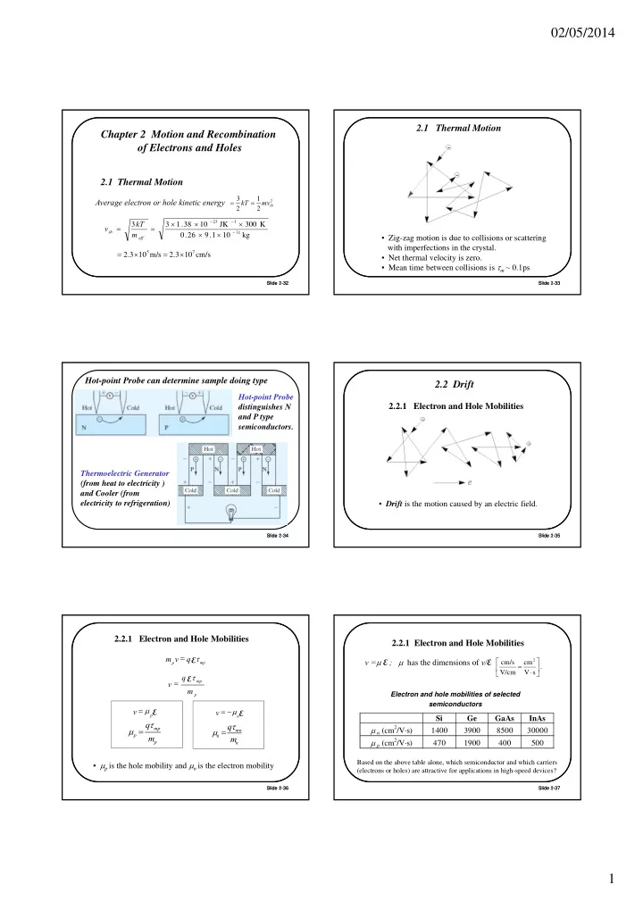
Slide 2-32
Chapter 2 Motion and Recombination
- f Electrons and Holes
2.1 Thermal Motion
Average electron or hole kinetic energy
2
2 1 2 3
th
mv kT
kg 10 1 . 9 26 . K 300 JK 10 38 . 1 3 3
31 1 23
eff th
m kT v cm/s 10 3 . 2 m/s 10 3 . 2
7 5
Slide 1-32 Slide 2-33
2.1 Thermal Motion
- Zig-zag motion is due to collisions or scattering
with imperfections in the crystal.
- Net thermal velocity is zero.
- Mean time between collisions is m ~ 0.1ps
Slide 1-33 Slide 2-34
Hot-point Probe can determine sample doing type
Thermoelectric Generator (from heat to electricity ) and Cooler (from electricity to refrigeration) Hot-point Probe distinguishes N and P type semiconductors.
Slide 1-34 Slide 2-35
2.2 Drift
2.2.1 Electron and Hole Mobilities
- Drift is the motion caused by an electric field.
Slide 1-35 Slide 2-36
2.2.1 Electron and Hole Mobilities
- p is the hole mobility and n is the electron mobility
mp p
q v m E
p mp
m q v E
p mp p
m q
n mn n
m q
E
p
v E
n
v
Slide 1-36 Slide 2-37
Electron and hole mobilities of selected semiconductors
2.2.1 Electron and Hole Mobilities
Si Ge GaAs InAs n (cm2/V·s) 1400 3900 8500 30000 p (cm2/V·s) 470 1900 400 500
. s V cm V/cm cm/s
2
v = E ; has the dimensions of v/E
Based on the above table alone, which semiconductor and which carriers (electrons or holes) are attractive for applications in high-speed devices?
Slide 1-37