
SLIDE 1
Fundamentals of Power Electronics Chapter 14: Transformer design
1
Chapter 14. Transformer Design
Some more advanced design issues, not considered in previous chapter:
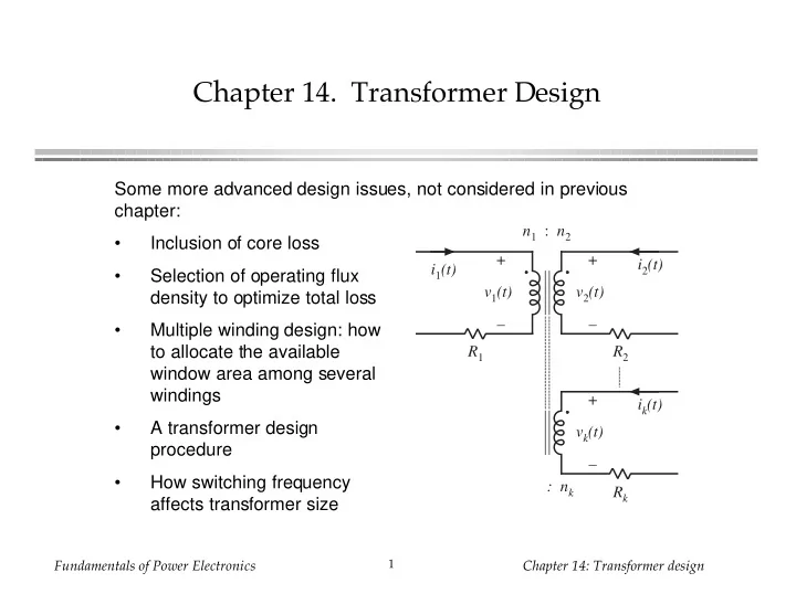
n1 : n2 : nk R1 R2 Rk + v1(t) – + v2(t) – + vk(t) – i1(t) i2(t) ik(t)
- Inclusion of core loss
- Selection of operating flux
density to optimize total loss
- Multiple winding design: how
to allocate the available window area among several windings
- A transformer design
procedure
- How switching frequency