
SLIDE 1
BJT amplifier: basic operation
0.2 0.4 0.6 0.8
IC IB IE αIE RC RC VB VB VCC Vo VCC t VBE IC IC t
- M. B. Patil, IIT Bombay
BJT amplifier: basic operation V CC I C I C R C V CC I C R C V o I E - - PowerPoint PPT Presentation
BJT amplifier: basic operation V CC I C I C R C V CC I C R C V o I E V B V B I B t I E 0 0.2 0.4 0.6 0.8 V BE t M. B. Patil, IIT Bombay BJT amplifier: basic operation V CC I C I C R C V CC I C R C V o I E V B V B I B t I E 0 0.2
BJT amplifier: basic operation
0.2 0.4 0.6 0.8
IC IB IE αIE RC RC VB VB VCC Vo VCC t VBE IC IC t
BJT amplifier: basic operation
0.2 0.4 0.6 0.8
IC IB IE αIE RC RC VB VB VCC Vo VCC t VBE IC IC t
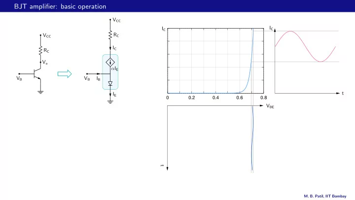
* In the active mode, IC changes exponentially with VBE : IC = αF IES [exp(VBE /VT ) − 1]
BJT amplifier: basic operation
0.2 0.4 0.6 0.8
IC IB IE αIE RC RC VB VB VCC Vo VCC t VBE IC IC t
* In the active mode, IC changes exponentially with VBE : IC = αF IES [exp(VBE /VT ) − 1] * Vo(t) = VCC − IC (t) RC ⇒ the amplitude of Vo, i.e., IC RC , can be made much larger than VB.
BJT amplifier: basic operation
0.2 0.4 0.6 0.8
IC IB IE αIE RC RC VB VB VCC Vo VCC t VBE IC IC t
* In the active mode, IC changes exponentially with VBE : IC = αF IES [exp(VBE /VT ) − 1] * Vo(t) = VCC − IC (t) RC ⇒ the amplitude of Vo, i.e., IC RC , can be made much larger than VB. * Note that both the input (VBE ) and output (Vo) voltages have DC (“bias”) components.
BJT amplifier: basic operation
0.6 0.7 50 40 30 20 10
1 1 2 2
IC IB IE αIE RC RC VB VB VCC Vo VCC IC (mA) t VBE (Volts) t
BJT amplifier: basic operation
0.6 0.7 50 40 30 20 10
1 1 2 2
IC IB IE αIE RC RC VB VB VCC Vo VCC IC (mA) t VBE (Volts) t * The gain depends on the DC (bias) value of VBE , the input voltage in this circuit.
BJT amplifier: basic operation
0.6 0.7 50 40 30 20 10
1 1 2 2
IC IB IE αIE RC RC VB VB VCC Vo VCC IC (mA) t VBE (Volts) t * The gain depends on the DC (bias) value of VBE , the input voltage in this circuit. * In practice, it is not possible to set the bias value
0.673 V).
BJT amplifier: basic operation
0.6 0.7 50 40 30 20 10
1 1 2 2
IC IB IE αIE RC RC VB VB VCC Vo VCC IC (mA) t VBE (Volts) t * The gain depends on the DC (bias) value of VBE , the input voltage in this circuit. * In practice, it is not possible to set the bias value
0.673 V). * Even if we could set the input bias as desired, device-to-device variation, change in temperature,
→ need a better biasing method.
BJT amplifier: basic operation
0.6 0.7 50 40 30 20 10
1 1 2 2
IC IB IE αIE RC RC VB VB VCC Vo VCC IC (mA) t VBE (Volts) t * The gain depends on the DC (bias) value of VBE , the input voltage in this circuit. * In practice, it is not possible to set the bias value
0.673 V). * Even if we could set the input bias as desired, device-to-device variation, change in temperature,
→ need a better biasing method. * Biasing the transistor at a specific VBE is equivalent to biasing it at a specific IC .
BJT amplifier biasing
B E C linear saturation 1 2 3 4 5 1 2 3 4 5
RB RC Vo VCC Vi 5 V IB2 IB3 IB4 IB5 IB1 Vo (Volts) Vi (Volts) VCE (Vo) VCC IC VCC/RC
Consider a more realistic BJT amplifier circuit, with RB added to limit the base current (and thus protect the transistor).
BJT amplifier biasing
B E C linear saturation 1 2 3 4 5 1 2 3 4 5
RB RC Vo VCC Vi 5 V IB2 IB3 IB4 IB5 IB1 Vo (Volts) Vi (Volts) VCE (Vo) VCC IC VCC/RC
Consider a more realistic BJT amplifier circuit, with RB added to limit the base current (and thus protect the transistor). * When Vi < 0.7 V, the B-E junction is not sufficiently forward biased, and the BJT is in the cut-off mode (VBE = Vi, VBC = Vi − VCC )
BJT amplifier biasing
B E C linear saturation 1 2 3 4 5 1 2 3 4 5
RB RC Vo VCC Vi 5 V IB2 IB3 IB4 IB5 IB1 Vo (Volts) Vi (Volts) VCE (Vo) VCC IC VCC/RC
Consider a more realistic BJT amplifier circuit, with RB added to limit the base current (and thus protect the transistor). * When Vi < 0.7 V, the B-E junction is not sufficiently forward biased, and the BJT is in the cut-off mode (VBE = Vi, VBC = Vi − VCC ) * When Vi exceeds 0.7 V, the BJT enters the linear region, and IB ≈ Vi − 0.7 RB . As Vi increases, IB and IC = βIB also increase, and Vo = VCC − IC RC falls.
BJT amplifier biasing
B E C linear saturation 1 2 3 4 5 1 2 3 4 5
RB RC Vo VCC Vi 5 V IB2 IB3 IB4 IB5 IB1 Vo (Volts) Vi (Volts) VCE (Vo) VCC IC VCC/RC
Consider a more realistic BJT amplifier circuit, with RB added to limit the base current (and thus protect the transistor). * When Vi < 0.7 V, the B-E junction is not sufficiently forward biased, and the BJT is in the cut-off mode (VBE = Vi, VBC = Vi − VCC ) * When Vi exceeds 0.7 V, the BJT enters the linear region, and IB ≈ Vi − 0.7 RB . As Vi increases, IB and IC = βIB also increase, and Vo = VCC − IC RC falls. * As Vi is increased further, Vo reaches V sat
CE (about 0.2 V), and the BJT enters the saturation region (both
B-E and B-C junctions are forward biased).
BJT amplifier biasing
B E C linear saturation 1 2 3 4 5 1 2 3 4 5
RB RC Vo VCC Vi 5 V IB2 IB3 IB4 IB5 IB1 Vo (Volts) Vi (Volts) VCE (Vo) VCC IC VCC/RC
BJT amplifier biasing
B E C linear saturation 1 2 3 4 5 1 2 3 4 5
RB RC Vo VCC Vi 5 V IB2 IB3 IB4 IB5 IB1 Vo (Volts) Vi (Volts) VCE (Vo) VCC IC VCC/RC
* The gain of the amplifier is given by dVo dVi .
BJT amplifier biasing
B E C linear saturation 1 2 3 4 5 1 2 3 4 5
RB RC Vo VCC Vi 5 V IB2 IB3 IB4 IB5 IB1 Vo (Volts) Vi (Volts) VCE (Vo) VCC IC VCC/RC
* The gain of the amplifier is given by dVo dVi . * Since Vo is nearly constant for Vi < 0.7 V (due to cut-off) and Vi > 1.3 V (due to saturation), the circuit will not work an an amplifier in this range.
BJT amplifier biasing
B E C linear saturation 1 2 3 4 5 1 2 3 4 5
RB RC Vo VCC Vi 5 V IB2 IB3 IB4 IB5 IB1 Vo (Volts) Vi (Volts) VCE (Vo) VCC IC VCC/RC
* The gain of the amplifier is given by dVo dVi . * Since Vo is nearly constant for Vi < 0.7 V (due to cut-off) and Vi > 1.3 V (due to saturation), the circuit will not work an an amplifier in this range. * Further, to get a large swing in Vo without distortion, the DC bias of Vi should be at the centre of the amplifying region, i.e., Vi ≈ 1 V .
BJT amplifier biasing
B E C B 1 2 3 4 5 1 2 3 4 5
RB RC Vo VCC Vi Vi Vo
BJT amplifier biasing
B E C B 1 2 3 4 5 1 2 3 4 5
RB RC Vo VCC Vi Vi Vo
t (msec) B 0.95 0.97 0.99 1.01 1.03 1.05 2.40 2.60 2.80 3.00 3.20 3.40 0.2 0.4 0.6 0.8 1
Vi Vo
BJT amplifier biasing
B E C B 1 2 3 4 5 1 2 3 4 5
RB RC Vo VCC Vi Vi Vo
t (msec) B 0.95 0.97 0.99 1.01 1.03 1.05 2.40 2.60 2.80 3.00 3.20 3.40 0.2 0.4 0.6 0.8 1
Vi Vo
A
BJT amplifier biasing
B E C B 1 2 3 4 5 1 2 3 4 5
RB RC Vo VCC Vi Vi Vo
t (msec) B 0.95 0.97 0.99 1.01 1.03 1.05 2.40 2.60 2.80 3.00 3.20 3.40 0.2 0.4 0.6 0.8 1
Vi Vo
A t (msec) A 4.50 4.60 4.70 4.80 4.90 5.00 0.70 0.72 0.74 0.76 0.78 0.80 0.2 0.4 0.6 0.8 1
Vi Vo
BJT amplifier biasing
B E C B 1 2 3 4 5 1 2 3 4 5
RB RC Vo VCC Vi Vi Vo
t (msec) B 0.95 0.97 0.99 1.01 1.03 1.05 2.40 2.60 2.80 3.00 3.20 3.40 0.2 0.4 0.6 0.8 1
Vi Vo
A t (msec) A 4.50 4.60 4.70 4.80 4.90 5.00 0.70 0.72 0.74 0.76 0.78 0.80 0.2 0.4 0.6 0.8 1
Vi Vo
C
BJT amplifier biasing
B E C B 1 2 3 4 5 1 2 3 4 5
RB RC Vo VCC Vi Vi Vo
t (msec) B 0.95 0.97 0.99 1.01 1.03 1.05 2.40 2.60 2.80 3.00 3.20 3.40 0.2 0.4 0.6 0.8 1
Vi Vo
A t (msec) A 4.50 4.60 4.70 4.80 4.90 5.00 0.70 0.72 0.74 0.76 0.78 0.80 0.2 0.4 0.6 0.8 1
Vi Vo
C t (msec) C 1.25 1.27 1.29 1.31 1.33 1.35 0.15 0.25 0.35 0.45 0.55 0.65 0.2 0.4 0.6 0.8 1
Vi Vo
(SEQUEL file: ee101 bjt amp1.sqproj)
BJT amplifier
B E C linear saturation 1 2 3 4 5 1 2 3 4 5
RB RC Vo VCC Vi 5 V IB2 IB3 IB4 IB5 IB1 Vo (Volts) Vi (Volts) VCE (Vo) VCC IC VCC/RC
* The key challenges in realizing this amplifier in practice are
BJT amplifier
B E C linear saturation 1 2 3 4 5 1 2 3 4 5
RB RC Vo VCC Vi 5 V IB2 IB3 IB4 IB5 IB1 Vo (Volts) Vi (Volts) VCE (Vo) VCC IC VCC/RC
* The key challenges in realizing this amplifier in practice are
certain bias value of VBE (or IC ).
BJT amplifier
B E C linear saturation 1 2 3 4 5 1 2 3 4 5
RB RC Vo VCC Vi 5 V IB2 IB3 IB4 IB5 IB1 Vo (Volts) Vi (Volts) VCE (Vo) VCC IC VCC/RC
* The key challenges in realizing this amplifier in practice are
certain bias value of VBE (or IC ).
BJT amplifier
B E C linear saturation 1 2 3 4 5 1 2 3 4 5
RB RC Vo VCC Vi 5 V IB2 IB3 IB4 IB5 IB1 Vo (Volts) Vi (Volts) VCE (Vo) VCC IC VCC/RC
* The key challenges in realizing this amplifier in practice are
certain bias value of VBE (or IC ).
* The first issue is addressed by using a suitable biasing scheme, and the second by using “coupling” capacitors.
BJT amplifier: a simple biasing scheme
B C E
VCC RB 15 V RC 1 k
“Biasing” an amplifier ⇒ selection of component values for a certain DC value of IC (or VBE ) (i.e., when no signal is applied).
BJT amplifier: a simple biasing scheme
B C E
VCC RB 15 V RC 1 k
“Biasing” an amplifier ⇒ selection of component values for a certain DC value of IC (or VBE ) (i.e., when no signal is applied). Equivalently, we may bias an amplifier for a certain DC value of VCE , since IC and VCE are related: VCE + IC RC = VCC .
BJT amplifier: a simple biasing scheme
B C E
VCC RB 15 V RC 1 k
“Biasing” an amplifier ⇒ selection of component values for a certain DC value of IC (or VBE ) (i.e., when no signal is applied). Equivalently, we may bias an amplifier for a certain DC value of VCE , since IC and VCE are related: VCE + IC RC = VCC . As an example, for RC = 1 k, β = 100, let us calculate RB for IC = 3.3 mA, assuming the BJT to be operating in the active mode.
BJT amplifier: a simple biasing scheme
B C E
VCC RB 15 V RC 1 k
“Biasing” an amplifier ⇒ selection of component values for a certain DC value of IC (or VBE ) (i.e., when no signal is applied). Equivalently, we may bias an amplifier for a certain DC value of VCE , since IC and VCE are related: VCE + IC RC = VCC . As an example, for RC = 1 k, β = 100, let us calculate RB for IC = 3.3 mA, assuming the BJT to be operating in the active mode. IB = IC β = 3.3 mA 100 = 33 µA = VCC − VBE RB = 15 − 0.7 RB
BJT amplifier: a simple biasing scheme
B C E
VCC RB 15 V RC 1 k
“Biasing” an amplifier ⇒ selection of component values for a certain DC value of IC (or VBE ) (i.e., when no signal is applied). Equivalently, we may bias an amplifier for a certain DC value of VCE , since IC and VCE are related: VCE + IC RC = VCC . As an example, for RC = 1 k, β = 100, let us calculate RB for IC = 3.3 mA, assuming the BJT to be operating in the active mode. IB = IC β = 3.3 mA 100 = 33 µA = VCC − VBE RB = 15 − 0.7 RB → RB = 14.3 V 33 µA = 430 kΩ .
BJT amplifier: a simple biasing scheme (continued)
B C E
VCC RB 15 V RC 1 k
With RB = 430 k, we expect IC = 3.3 mA, assuming β = 100.
BJT amplifier: a simple biasing scheme (continued)
B C E
VCC RB 15 V RC 1 k
With RB = 430 k, we expect IC = 3.3 mA, assuming β = 100. However, in practice, there is a substantial variation in the β value (even for the same transistor type). The manufacturer may specify the nominal value of β as 100, but the actual value may be 150, for example.
BJT amplifier: a simple biasing scheme (continued)
B C E
VCC RB 15 V RC 1 k
With RB = 430 k, we expect IC = 3.3 mA, assuming β = 100. However, in practice, there is a substantial variation in the β value (even for the same transistor type). The manufacturer may specify the nominal value of β as 100, but the actual value may be 150, for example. With β = 150, the actual IC is, IC = β × VCC − VBE RB = 150 × (15 − 0.7) V 430 k = 5 mA , which is significantly different than the intended value, viz., 3.3 mA.
BJT amplifier: a simple biasing scheme (continued)
B C E
VCC RB 15 V RC 1 k
With RB = 430 k, we expect IC = 3.3 mA, assuming β = 100. However, in practice, there is a substantial variation in the β value (even for the same transistor type). The manufacturer may specify the nominal value of β as 100, but the actual value may be 150, for example. With β = 150, the actual IC is, IC = β × VCC − VBE RB = 150 × (15 − 0.7) V 430 k = 5 mA , which is significantly different than the intended value, viz., 3.3 mA. → need a biasing scheme which is not so sensitive to β.
BJT amplifier: improved biasing scheme
IE IB IC 10 V 10 k 2.2 k 3.6 k 1 k RE RC R2 R1 VCC
BJT amplifier: improved biasing scheme
IE IB IC 10 V 10 k 2.2 k 3.6 k 1 k RE RC R2 R1 VCC IE IB IC RE RC R2 R1 VCC VCC
BJT amplifier: improved biasing scheme
IE IB IC 10 V 10 k 2.2 k 3.6 k 1 k RE RC R2 R1 VCC IE IB IC RE RC R2 R1 VCC VCC IE IB IC RE RC RTh VTh VCC
BJT amplifier: improved biasing scheme
IE IB IC 10 V 10 k 2.2 k 3.6 k 1 k RE RC R2 R1 VCC IE IB IC RE RC R2 R1 VCC VCC IE IB IC RE RC RTh VTh VCC
VTh = R2 R1 + R2 VCC = 2.2 k 10 k + 2.2 k × 10 V = 1.8 V , RTh = R1 R2 = 1.8 k
BJT amplifier: improved biasing scheme
IE IB IC 10 V 10 k 2.2 k 3.6 k 1 k RE RC R2 R1 VCC IE IB IC RE RC R2 R1 VCC VCC IE IB IC RE RC RTh VTh VCC
VTh = R2 R1 + R2 VCC = 2.2 k 10 k + 2.2 k × 10 V = 1.8 V , RTh = R1 R2 = 1.8 k Assuming the BJT to be in the active mode, KVL: VTh = RTh IB + VBE + RE IE = RTh IB + VBE + (β + 1) IB RE
BJT amplifier: improved biasing scheme
IE IB IC 10 V 10 k 2.2 k 3.6 k 1 k RE RC R2 R1 VCC IE IB IC RE RC R2 R1 VCC VCC IE IB IC RE RC RTh VTh VCC
VTh = R2 R1 + R2 VCC = 2.2 k 10 k + 2.2 k × 10 V = 1.8 V , RTh = R1 R2 = 1.8 k Assuming the BJT to be in the active mode, KVL: VTh = RTh IB + VBE + RE IE = RTh IB + VBE + (β + 1) IB RE → IB = VTh − VBE RTh + (β + 1) RE , IC = β IB = β (VTh − VBE ) RTh + (β + 1) RE .
BJT amplifier: improved biasing scheme
IE IB IC 10 V 10 k 2.2 k 3.6 k 1 k RE RC R2 R1 VCC IE IB IC RE RC R2 R1 VCC VCC IE IB IC RE RC RTh VTh VCC
VTh = R2 R1 + R2 VCC = 2.2 k 10 k + 2.2 k × 10 V = 1.8 V , RTh = R1 R2 = 1.8 k Assuming the BJT to be in the active mode, KVL: VTh = RTh IB + VBE + RE IE = RTh IB + VBE + (β + 1) IB RE → IB = VTh − VBE RTh + (β + 1) RE , IC = β IB = β (VTh − VBE ) RTh + (β + 1) RE . For β = 100, IC =1.07 mA.
BJT amplifier: improved biasing scheme
IE IB IC 10 V 10 k 2.2 k 3.6 k 1 k RE RC R2 R1 VCC IE IB IC RE RC R2 R1 VCC VCC IE IB IC RE RC RTh VTh VCC
VTh = R2 R1 + R2 VCC = 2.2 k 10 k + 2.2 k × 10 V = 1.8 V , RTh = R1 R2 = 1.8 k Assuming the BJT to be in the active mode, KVL: VTh = RTh IB + VBE + RE IE = RTh IB + VBE + (β + 1) IB RE → IB = VTh − VBE RTh + (β + 1) RE , IC = β IB = β (VTh − VBE ) RTh + (β + 1) RE . For β = 100, IC =1.07 mA. For β = 200, IC =1.085 mA.
BJT amplifier: improved biasing scheme (continued)
IE IB IC 10 V 10 k 2.2 k 3.6 k 1 k RE RC R2 R1 VCC
With IC = 1.1 mA, the various DC (“bias”) voltages are
BJT amplifier: improved biasing scheme (continued)
IE IB IC 10 V 10 k 2.2 k 3.6 k 1 k RE RC R2 R1 VCC
With IC = 1.1 mA, the various DC (“bias”) voltages are VE = IE RE ≈ 1.1 mA × 1 k = 1.1 V ,
BJT amplifier: improved biasing scheme (continued)
IE IB IC 10 V 10 k 2.2 k 3.6 k 1 k RE RC R2 R1 VCC 1.1 V
With IC = 1.1 mA, the various DC (“bias”) voltages are VE = IE RE ≈ 1.1 mA × 1 k = 1.1 V ,
BJT amplifier: improved biasing scheme (continued)
IE IB IC 10 V 10 k 2.2 k 3.6 k 1 k RE RC R2 R1 VCC 1.1 V
With IC = 1.1 mA, the various DC (“bias”) voltages are VE = IE RE ≈ 1.1 mA × 1 k = 1.1 V , VB = VE + VBE ≈ 1.1 V + 0.7 V = 1.8 V ,
BJT amplifier: improved biasing scheme (continued)
IE IB IC 10 V 10 k 2.2 k 3.6 k 1 k RE RC R2 R1 VCC 1.1 V 1.8 V
With IC = 1.1 mA, the various DC (“bias”) voltages are VE = IE RE ≈ 1.1 mA × 1 k = 1.1 V , VB = VE + VBE ≈ 1.1 V + 0.7 V = 1.8 V ,
BJT amplifier: improved biasing scheme (continued)
IE IB IC 10 V 10 k 2.2 k 3.6 k 1 k RE RC R2 R1 VCC 1.1 V 1.8 V
With IC = 1.1 mA, the various DC (“bias”) voltages are VE = IE RE ≈ 1.1 mA × 1 k = 1.1 V , VB = VE + VBE ≈ 1.1 V + 0.7 V = 1.8 V , VC = VCC − IC RC = 10 V − 1.1 mA × 3.6 k ≈ 6 V ,
BJT amplifier: improved biasing scheme (continued)
IE IB IC 10 V 10 k 2.2 k 3.6 k 1 k RE RC R2 R1 VCC 1.1 V 1.8 V 6 V
With IC = 1.1 mA, the various DC (“bias”) voltages are VE = IE RE ≈ 1.1 mA × 1 k = 1.1 V , VB = VE + VBE ≈ 1.1 V + 0.7 V = 1.8 V , VC = VCC − IC RC = 10 V − 1.1 mA × 3.6 k ≈ 6 V ,
BJT amplifier: improved biasing scheme (continued)
IE IB IC 10 V 10 k 2.2 k 3.6 k 1 k RE RC R2 R1 VCC 1.1 V 1.8 V 6 V
With IC = 1.1 mA, the various DC (“bias”) voltages are VE = IE RE ≈ 1.1 mA × 1 k = 1.1 V , VB = VE + VBE ≈ 1.1 V + 0.7 V = 1.8 V , VC = VCC − IC RC = 10 V − 1.1 mA × 3.6 k ≈ 6 V , VCE = VC − VE = 6 − 1.1 = 4.9 V .
BJT amplifier: improved biasing scheme (continued)
IE IB IC 10 V 10 k 2.2 k 3.6 k 1 k RE RC R2 R1 VCC
A quick estimate of the bias values can be obtained by ignoring IB (which is fair if β is large). In that case,
BJT amplifier: improved biasing scheme (continued)
IE IB IC 10 V 10 k 2.2 k 3.6 k 1 k RE RC R2 R1 VCC
A quick estimate of the bias values can be obtained by ignoring IB (which is fair if β is large). In that case, VB = R2 R1 + R2 VCC = 2.2 k 10 k + 2.2 k × 10 V = 1.8 V .
BJT amplifier: improved biasing scheme (continued)
IE IB IC 10 V 10 k 2.2 k 3.6 k 1 k RE RC R2 R1 VCC
A quick estimate of the bias values can be obtained by ignoring IB (which is fair if β is large). In that case, VB = R2 R1 + R2 VCC = 2.2 k 10 k + 2.2 k × 10 V = 1.8 V . VE = VB − VBE ≈ 1.8 V − 0.7 V = 1.1 V .
BJT amplifier: improved biasing scheme (continued)
IE IB IC 10 V 10 k 2.2 k 3.6 k 1 k RE RC R2 R1 VCC
A quick estimate of the bias values can be obtained by ignoring IB (which is fair if β is large). In that case, VB = R2 R1 + R2 VCC = 2.2 k 10 k + 2.2 k × 10 V = 1.8 V . VE = VB − VBE ≈ 1.8 V − 0.7 V = 1.1 V . IE = VE RE = 1.1 V 1 k = 1.1 mA.
BJT amplifier: improved biasing scheme (continued)
IE IB IC 10 V 10 k 2.2 k 3.6 k 1 k RE RC R2 R1 VCC
A quick estimate of the bias values can be obtained by ignoring IB (which is fair if β is large). In that case, VB = R2 R1 + R2 VCC = 2.2 k 10 k + 2.2 k × 10 V = 1.8 V . VE = VB − VBE ≈ 1.8 V − 0.7 V = 1.1 V . IE = VE RE = 1.1 V 1 k = 1.1 mA. IC = α IE ≈ IE = 1.1 mA.
BJT amplifier: improved biasing scheme (continued)
IE IB IC 10 V 10 k 2.2 k 3.6 k 1 k RE RC R2 R1 VCC
A quick estimate of the bias values can be obtained by ignoring IB (which is fair if β is large). In that case, VB = R2 R1 + R2 VCC = 2.2 k 10 k + 2.2 k × 10 V = 1.8 V . VE = VB − VBE ≈ 1.8 V − 0.7 V = 1.1 V . IE = VE RE = 1.1 V 1 k = 1.1 mA. IC = α IE ≈ IE = 1.1 mA. VCE = VCC − IC RC − IE RE = 10 V − (3.6 k × 1.1 mA) − (1 k × 1.1 mA) ≈ 5 V .
Adding signal to bias
vB RC R1 R2 RE VCC
Adding signal to bias
vB RC R1 R2 RE VCC
* As we have seen earlier, the input signal vs(t) = V sin ωt (for example) needs to be mixed with the desired bias value VB so that the net voltage at the base is vB(t) = VB + V sin ωt.
Adding signal to bias
vB RC R1 R2 RE VCC CB vs
* As we have seen earlier, the input signal vs(t) = V sin ωt (for example) needs to be mixed with the desired bias value VB so that the net voltage at the base is vB(t) = VB + V sin ωt. * This can be achieved by using a coupling capacitor CB.
Adding signal to bias
vB RC R1 R2 RE VCC CB vs
* As we have seen earlier, the input signal vs(t) = V sin ωt (for example) needs to be mixed with the desired bias value VB so that the net voltage at the base is vB(t) = VB + V sin ωt. * This can be achieved by using a coupling capacitor CB. * Let us consider a simple circuit to illustrate how a coupling capacitor works.
RC circuit with DC + AC sources
A
R2 vC R1 vA Vmsin ωt vs(t) V0 (DC)
We are interested in the solution (currents and voltages) in the “sinusoidal steady state” when the exponential transients have vanished and each quantity x(t) is of the form X0 (constant) + Xm sin(ωt + α).
RC circuit with DC + AC sources
A
R2 vC R1 vA Vmsin ωt vs(t) V0 (DC)
We are interested in the solution (currents and voltages) in the “sinusoidal steady state” when the exponential transients have vanished and each quantity x(t) is of the form X0 (constant) + Xm sin(ωt + α). There are two ways to obtain the solution:
RC circuit with DC + AC sources
A
R2 vC R1 vA Vmsin ωt vs(t) V0 (DC)
We are interested in the solution (currents and voltages) in the “sinusoidal steady state” when the exponential transients have vanished and each quantity x(t) is of the form X0 (constant) + Xm sin(ωt + α). There are two ways to obtain the solution: (1) Solve the circuit equations directly: vA(t) R1 + vA(t) − V0 R2 = C d dt (vs(t) − vA(t)) .
RC circuit with DC + AC sources
A
R2 vC R1 vA Vmsin ωt vs(t) V0 (DC)
We are interested in the solution (currents and voltages) in the “sinusoidal steady state” when the exponential transients have vanished and each quantity x(t) is of the form X0 (constant) + Xm sin(ωt + α). There are two ways to obtain the solution: (1) Solve the circuit equations directly: vA(t) R1 + vA(t) − V0 R2 = C d dt (vs(t) − vA(t)) . (2) Use the DC circuit + AC circuit approach.
Resistor in sinusoidal steady state
iR(t) vR(t) R
Resistor in sinusoidal steady state
iR(t) vR(t) R Let vR(t) = VR + vr(t) where VR = constant, vr(t) = VR sin (ωt + α), iR(t) = IR + ir(t) where IR = constant, ir(t) = IR sin (ωt + α).
Resistor in sinusoidal steady state
iR(t) vR(t) R Let vR(t) = VR + vr(t) where VR = constant, vr(t) = VR sin (ωt + α), iR(t) = IR + ir(t) where IR = constant, ir(t) = IR sin (ωt + α). Since vR(t) = R × iR(t), we get [VR + vr(t)] = R × [IR + ir(t)].
Resistor in sinusoidal steady state
iR(t) vR(t) R Let vR(t) = VR + vr(t) where VR = constant, vr(t) = VR sin (ωt + α), iR(t) = IR + ir(t) where IR = constant, ir(t) = IR sin (ωt + α). Since vR(t) = R × iR(t), we get [VR + vr(t)] = R × [IR + ir(t)]. This relationship can be split into two: VR = R × IR, and vr(t) = R × ir(t).
Resistor in sinusoidal steady state
iR(t) vR(t) R Let vR(t) = VR + vr(t) where VR = constant, vr(t) = VR sin (ωt + α), iR(t) = IR + ir(t) where IR = constant, ir(t) = IR sin (ωt + α). Since vR(t) = R × iR(t), we get [VR + vr(t)] = R × [IR + ir(t)]. This relationship can be split into two: VR = R × IR, and vr(t) = R × ir(t). In other words, a resistor can be described by R ir(t) vr(t) DC AC R IR VR
Capacitor in sinusoidal steady state
C iC(t) vC(t)
Capacitor in sinusoidal steady state
C iC(t) vC(t) Let vC (t) = VC + vc(t) where VC = constant, vc(t) = VC sin (ωt + α), iC (t) = IC + ic(t) where IC = constant, ic(t) = IC sin (ωt + β).
Capacitor in sinusoidal steady state
C iC(t) vC(t) Let vC (t) = VC + vc(t) where VC = constant, vc(t) = VC sin (ωt + α), iC (t) = IC + ic(t) where IC = constant, ic(t) = IC sin (ωt + β). Since iC (t) = C dvC dt , we get [IC + ic(t)] = C d dt (VC + vc(t)).
Capacitor in sinusoidal steady state
C iC(t) vC(t) Let vC (t) = VC + vc(t) where VC = constant, vc(t) = VC sin (ωt + α), iC (t) = IC + ic(t) where IC = constant, ic(t) = IC sin (ωt + β). Since iC (t) = C dvC dt , we get [IC + ic(t)] = C d dt (VC + vc(t)). This relationship can be split into two: IC = C dVC dt = 0, and ic(t) = C dvc dt .
Capacitor in sinusoidal steady state
C iC(t) vC(t) Let vC (t) = VC + vc(t) where VC = constant, vc(t) = VC sin (ωt + α), iC (t) = IC + ic(t) where IC = constant, ic(t) = IC sin (ωt + β). Since iC (t) = C dvC dt , we get [IC + ic(t)] = C d dt (VC + vc(t)). This relationship can be split into two: IC = C dVC dt = 0, and ic(t) = C dvc dt . In other words, a capacitor can be described by IC ic(t) AC DC VC vc(t) C
Voltage sources in sinusoidal steady state
DC voltage source: is(t) vs(t) IS VS iS(t) vS(t) DC AC vS(t) = VS + 0
Voltage sources in sinusoidal steady state
DC voltage source: is(t) vs(t) IS VS iS(t) vS(t) DC AC vS(t) = VS + 0 AC voltage source: is(t) vs(t) IS VS iS(t) vS(t) DC AC vS(t) = 0 + vs(t)
RC circuit with DC + AC sources
DC circuit AC circuit A A A
R2 R2 R2 vC R1 vA VC R1 VA vc R1 va Vmsin ωt Vmsin ωt vs(t) vs(t) V0 (DC) V0
RC circuit with DC + AC sources
DC circuit AC circuit A A A
R2 R2 R2 vC R1 vA VC R1 VA vc R1 va Vmsin ωt Vmsin ωt vs(t) vs(t) V0 (DC) V0 DC circuit: VA R1 + VA − V0 R2 = 0. (1)
RC circuit with DC + AC sources
DC circuit AC circuit A A A
R2 R2 R2 vC R1 vA VC R1 VA vc R1 va Vmsin ωt Vmsin ωt vs(t) vs(t) V0 (DC) V0 DC circuit: VA R1 + VA − V0 R2 = 0. (1) AC circuit: va R1 + va R2 = C d dt (vs − va). (2)
RC circuit with DC + AC sources
DC circuit AC circuit A A A
R2 R2 R2 vC R1 vA VC R1 VA vc R1 va Vmsin ωt Vmsin ωt vs(t) vs(t) V0 (DC) V0 DC circuit: VA R1 + VA − V0 R2 = 0. (1) AC circuit: va R1 + va R2 = C d dt (vs − va). (2) Adding (1) and (2), we get VA + va R1 + VA + va − V0 R2 = C d dt (vs − va). (3)
RC circuit with DC + AC sources
DC circuit AC circuit A A A
R2 R2 R2 vC R1 vA VC R1 VA vc R1 va Vmsin ωt Vmsin ωt vs(t) vs(t) V0 (DC) V0 DC circuit: VA R1 + VA − V0 R2 = 0. (1) AC circuit: va R1 + va R2 = C d dt (vs − va). (2) Adding (1) and (2), we get VA + va R1 + VA + va − V0 R2 = C d dt (vs − va). (3) Compare with the equation obtained directly from the original circuit: vA R1 + vA − V0 R2 = C d dt (vs − vA). (4)
→ Instead of computing vA(t) directly, we can compute VA and va(t) separately, and then use vA(t) = VA + va(t).
Common-emitter amplifier
bypass capacitor load resistor coupling capacitor coupling capacitor
vs CB CC CE VCC RL RE R2 R1 RC
Common-emitter amplifier
bypass capacitor load resistor coupling capacitor coupling capacitor
vs CB CC CE VCC RL RE R2 R1 RC DC circuit VCC RE R2 R1 RC
Common-emitter amplifier
bypass capacitor load resistor coupling capacitor coupling capacitor
vs CB CC CE VCC RL RE R2 R1 RC DC circuit VCC RE R2 R1 RC AND AC circuit CB CC CE RL RE R2 vs R1 RC
Common-emitter amplifier
bypass capacitor load resistor coupling capacitor coupling capacitor
vs CB CC CE VCC RL RE R2 R1 RC DC circuit VCC RE R2 R1 RC AND AC circuit CB CC CE RL RE R2 vs R1 RC
* The coupling capacitors ensure that the signal source and the load resistor do not affect the DC bias of the amplifier. (We will see the purpose of CE a little later.)
Common-emitter amplifier
bypass capacitor load resistor coupling capacitor coupling capacitor
vs CB CC CE VCC RL RE R2 R1 RC DC circuit VCC RE R2 R1 RC AND AC circuit CB CC CE RL RE R2 vs R1 RC
* The coupling capacitors ensure that the signal source and the load resistor do not affect the DC bias of the amplifier. (We will see the purpose of CE a little later.) * This enables us to bias the amplifier without worrying about what load it is going to drive.
Common-emitter amplifier: AC circuit
CB CC CE RL RE R2 vs R1 RC
Common-emitter amplifier: AC circuit
CB CC CE RL RE R2 vs R1 RC
* The coupling and bypass capacitors are “large” (typically, a few µF), and at frequencies of interest, their impedance is small. For example, for C = 10 µF, f = 1 kHz, ZC = 1 2π × 103 × 10 × 10−6 = 16 Ω, which is much smaller than typical values of R1, R2, RC , RE (a few kΩ). ⇒ CB, CC , CE can be replaced by short circuits at the frequencies of interest.
Common-emitter amplifier: AC circuit
CB CC CE RL RE R2 vs R1 RC RL R2 vs R1 RC
* The coupling and bypass capacitors are “large” (typically, a few µF), and at frequencies of interest, their impedance is small. For example, for C = 10 µF, f = 1 kHz, ZC = 1 2π × 103 × 10 × 10−6 = 16 Ω, which is much smaller than typical values of R1, R2, RC , RE (a few kΩ). ⇒ CB, CC , CE can be replaced by short circuits at the frequencies of interest. * The circuit can be re-drawn in a more friendly format.
Common-emitter amplifier: AC circuit
CB CC CE RL RE R2 vs R1 RC RL R2 vs R1 RC RL vs R2 R1 RC
* The coupling and bypass capacitors are “large” (typically, a few µF), and at frequencies of interest, their impedance is small. For example, for C = 10 µF, f = 1 kHz, ZC = 1 2π × 103 × 10 × 10−6 = 16 Ω, which is much smaller than typical values of R1, R2, RC , RE (a few kΩ). ⇒ CB, CC , CE can be replaced by short circuits at the frequencies of interest. * The circuit can be re-drawn in a more friendly format. * We now need to figure out the AC description of a BJT.
BJT: AC model
B E C
0.2 0.4 0.6 0.8 1 1.1 0.9 0.7 0.5 t (msec)
iC (mA) vBE iC iE iB f = 1 kHz V0 = 0.65 V, vBE(t) = V0 + Vm sin ωt Vm = 10 mV Vm = 5 mV Vm = 2 mV
BJT: AC model
B E C
0.2 0.4 0.6 0.8 1 1.1 0.9 0.7 0.5 t (msec)
iC (mA) vBE iC iE iB f = 1 kHz V0 = 0.65 V, vBE(t) = V0 + Vm sin ωt Vm = 10 mV Vm = 5 mV Vm = 2 mV
* As the vBE amplitude increases, the shape of iC (t) deviates from a sinusoid → distortion.
BJT: AC model
B E C
0.2 0.4 0.6 0.8 1 1.1 0.9 0.7 0.5 t (msec)
iC (mA) vBE iC iE iB f = 1 kHz V0 = 0.65 V, vBE(t) = V0 + Vm sin ωt Vm = 10 mV Vm = 5 mV Vm = 2 mV
* As the vBE amplitude increases, the shape of iC (t) deviates from a sinusoid → distortion. * If vbe(t), i.e., the time-varying part of vBE , is kept small, iC varies linearly with vBE . How small? Let us look at this in more detail.
BJT: small-signal model
B E C B C E
0.2 0.4 0.6 0.8 1 1.1 0.9 0.7 0.5 t (msec)
αIE vBE vBE iB iC iE iE iC iB iC (mA) f = 1 kHz V0 = 0.65 V, vBE(t) = V0 + Vm sin ωt Vm = 10 mV Vm = 5 mV Vm = 2 mV Let vBE (t) = VBE + vbe(t) (bias+signal), and iC (t) = IC + ic(t).
BJT: small-signal model
B E C B C E
0.2 0.4 0.6 0.8 1 1.1 0.9 0.7 0.5 t (msec)
αIE vBE vBE iB iC iE iE iC iB iC (mA) f = 1 kHz V0 = 0.65 V, vBE(t) = V0 + Vm sin ωt Vm = 10 mV Vm = 5 mV Vm = 2 mV Let vBE (t) = VBE + vbe(t) (bias+signal), and iC (t) = IC + ic(t). Assuming active mode, iC (t) = α iE (t) = α IES
vBE (t) VT
Since the B-E junction is forward-biased, exp vBE (t) VT
iC (t) = α IES exp vBE (t) VT
VBE + vbe(t) VT
VBE VT
vbe(t) VT
If vbe(t) = 0, iC (t) = IC (the bias value of iC ), i.e., IC = α IES exp VBE VT
vbe(t) VT
BJT: small-signal model
B E C B C E
0.2 0.4 0.6 0.8 1 1.1 0.9 0.7 0.5 t (msec)
αIE vBE vBE iB iC iE iE iC iB iC (mA) f = 1 kHz V0 = 0.65 V, vBE(t) = V0 + Vm sin ωt Vm = 10 mV Vm = 5 mV Vm = 2 mV iC (t) = IC exp vbe(t) VT
2 + · · ·
x = vbe(t)/VT .
BJT: small-signal model
B E C B C E
0.2 0.4 0.6 0.8 1 1.1 0.9 0.7 0.5 t (msec)
αIE vBE vBE iB iC iE iE iC iB iC (mA) f = 1 kHz V0 = 0.65 V, vBE(t) = V0 + Vm sin ωt Vm = 10 mV Vm = 5 mV Vm = 2 mV iC (t) = IC exp vbe(t) VT
2 + · · ·
x = vbe(t)/VT . If x is small, i.e., if the amplitude of vbe(t) is small compared to the thermal voltage VT , we get iC (t) = IC
VT
We can now see that, for |vbe(t)| ≪ VT , the relationship between iC (t) and vbe(t) is linear, as we have observed previously.
BJT: small-signal model
B E C B C E
0.2 0.4 0.6 0.8 1 1.1 0.9 0.7 0.5 t (msec)
αIE vBE vBE iB iC iE iE iC iB iC (mA) f = 1 kHz V0 = 0.65 V, vBE(t) = V0 + Vm sin ωt Vm = 10 mV Vm = 5 mV Vm = 2 mV iC (t) = IC exp vbe(t) VT
2 + · · ·
x = vbe(t)/VT . If x is small, i.e., if the amplitude of vbe(t) is small compared to the thermal voltage VT , we get iC (t) = IC
VT
We can now see that, for |vbe(t)| ≪ VT , the relationship between iC (t) and vbe(t) is linear, as we have observed previously. iC (t) = IC + ic(t) = IC
VT
ic(t) = IC VT vbe(t)
BJT: small-signal model
B E C B C E B C E
αIE vbe vBE vBE iB iC iE ib ic ie iE iC iB gmvbe rπ
The relationship, ic(t) = IC VT vbe(t) can be represented by a VCCS, ic(t) = gm vbe(t), where gm = IC /VT is the “transconductance.”
BJT: small-signal model
B E C B C E B C E
αIE vbe vBE vBE iB iC iE ib ic ie iE iC iB gmvbe rπ
The relationship, ic(t) = IC VT vbe(t) can be represented by a VCCS, ic(t) = gm vbe(t), where gm = IC /VT is the “transconductance.” For the base current, we have, iB(t) = IB + ib(t) = 1 β [IC + ic(t)] → ib(t) = 1 β ic(t) = 1 β gm vbe(t) → vbe(t) = (β/gm) ib(t).
BJT: small-signal model
B E C B C E B C E
αIE vbe vBE vBE iB iC iE ib ic ie iE iC iB gmvbe rπ
The relationship, ic(t) = IC VT vbe(t) can be represented by a VCCS, ic(t) = gm vbe(t), where gm = IC /VT is the “transconductance.” For the base current, we have, iB(t) = IB + ib(t) = 1 β [IC + ic(t)] → ib(t) = 1 β ic(t) = 1 β gm vbe(t) → vbe(t) = (β/gm) ib(t). The above relationship is represented by a resistance, rπ = β/gm, connected between B and E.
BJT: small-signal model
B E C B C E B C E
αIE vbe vBE vBE iB iC iE ib ic ie iE iC iB gmvbe rπ
The relationship, ic(t) = IC VT vbe(t) can be represented by a VCCS, ic(t) = gm vbe(t), where gm = IC /VT is the “transconductance.” For the base current, we have, iB(t) = IB + ib(t) = 1 β [IC + ic(t)] → ib(t) = 1 β ic(t) = 1 β gm vbe(t) → vbe(t) = (β/gm) ib(t). The above relationship is represented by a resistance, rπ = β/gm, connected between B and E. The resulting model is called the π-model for small-signal description of a BJT.
BJT: small-signal model
B E C B C E B C E
αIE vbe vBE vBE iB iC iE ib ic ie iE iC iB gmvbe rπ
* The transconductance gm depends on the biasing of the BJT, since gm = IC /VT . For IC = 1 mA, VT ≈ 25 mV (room temperature), gm = 1 mA/25 mV = 40 m℧ (milli-mho or milli-siemens).
BJT: small-signal model
B E C B C E B C E
αIE vbe vBE vBE iB iC iE ib ic ie iE iC iB gmvbe rπ
* The transconductance gm depends on the biasing of the BJT, since gm = IC /VT . For IC = 1 mA, VT ≈ 25 mV (room temperature), gm = 1 mA/25 mV = 40 m℧ (milli-mho or milli-siemens). * rπ also depends on IC , since rπ = β/gm = β VT /IC . For IC = 1 mA, VT ≈ 25 mV , β = 100, rπ = 2.5 kΩ.
BJT: small-signal model
B E C B C E B C E
αIE vbe vBE vBE iB iC iE ib ic ie iE iC iB gmvbe rπ
* The transconductance gm depends on the biasing of the BJT, since gm = IC /VT . For IC = 1 mA, VT ≈ 25 mV (room temperature), gm = 1 mA/25 mV = 40 m℧ (milli-mho or milli-siemens). * rπ also depends on IC , since rπ = β/gm = β VT /IC . For IC = 1 mA, VT ≈ 25 mV , β = 100, rπ = 2.5 kΩ. * Note that the small-signal model is valid only for small vbe (small compared to VT ).
BJT: small-signal model
B E C B C E
vbe vBE iB iC iE ib ic ie gmvbe rπ
* In the above model, note that ic is independent of vce.
BJT: small-signal model
B E C B C E
vbe vBE iB iC iE ib ic ie gmvbe rπ
1 2 3 4 5 1
IC (mA) VCE (V)
* In the above model, note that ic is independent of vce. * In practice, ic does depend on vce because of the Early effect, and dIC dVCE ≈ constant = 1/ro, where ro is called the output resistance.
BJT: small-signal model
B E C B C E
vbe vBE iB iC iE ib ic ie gmvbe rπ
1 2 3 4 5 1
IC (mA) VCE (V)
* In the above model, note that ic is independent of vce. * In practice, ic does depend on vce because of the Early effect, and dIC dVCE ≈ constant = 1/ro, where ro is called the output resistance. * A more accurate model includes ro as well.
BJT: small-signal model
B E C B C E
vbe vBE iB iC iE ib ic ie gmvbe rπ
1 2 3 4 5 1
IC (mA) VCE (V)
B C E
ro vbe ib ie ic gmvbe rπ
* In the above model, note that ic is independent of vce. * In practice, ic does depend on vce because of the Early effect, and dIC dVCE ≈ constant = 1/ro, where ro is called the output resistance. * A more accurate model includes ro as well.
BJT: small-signal model
C B E
ro vbe ie ic ib Cπ Cµ rb gmvbe rπ
n+ p+ substrate n+ buried layer substrate contact n+ p+ epi-layer insulator p n contact base contact emitter contact collector ∼ 5 µm > 250 µm p+
* A few other components are required to make the small-signal model complete: rb: base spreading resistance Cπ: base charging capacitance + B-E junction capacitance Cµ: B-C junction capacitance
BJT: small-signal model
C B E
ro vbe ie ic ib Cπ Cµ rb gmvbe rπ
n+ p+ substrate n+ buried layer substrate contact n+ p+ epi-layer insulator p n contact base contact emitter contact collector ∼ 5 µm > 250 µm p+
* A few other components are required to make the small-signal model complete: rb: base spreading resistance Cπ: base charging capacitance + B-E junction capacitance Cµ: B-C junction capacitance * The capacitances are typically in the pF range. At low frequencies, 1/ωC is large, and the capacitances can be replaced by open circuits.
BJT: small-signal model
C B E
ro vbe ie ic ib Cπ Cµ rb gmvbe rπ
n+ p+ substrate n+ buried layer substrate contact n+ p+ epi-layer insulator p n contact base contact emitter contact collector ∼ 5 µm > 250 µm p+
* A few other components are required to make the small-signal model complete: rb: base spreading resistance Cπ: base charging capacitance + B-E junction capacitance Cµ: B-C junction capacitance * The capacitances are typically in the pF range. At low frequencies, 1/ωC is large, and the capacitances can be replaced by open circuits. * Note that the small-signal models we have described are valid in the active region only.
Common-emitter amplifier
bypass capacitor load resistor coupling capacitor coupling capacitor
AND DC circuit AC circuit vs CB CC CB CC CE CE VCC VCC RL RL RE RE RE R2 R2 R2 vs R1 R1 R1 RC RC RC 6 V 1.1 V 1.8 V 2.2 k 3.6 k 1 k 10 k 10 V * We have already analysed the DC (bias) circuit of this amplifier and found that VB = 1.8 V , VE = 1.1 V , VC = 6 V , and IC = 1.1 mA.
Common-emitter amplifier
bypass capacitor load resistor coupling capacitor coupling capacitor
AND DC circuit AC circuit vs CB CC CB CC CE CE VCC VCC RL RL RE RE RE R2 R2 R2 vs R1 R1 R1 RC RC RC 6 V 1.1 V 1.8 V 2.2 k 3.6 k 1 k 10 k 10 V * We have already analysed the DC (bias) circuit of this amplifier and found that VB = 1.8 V , VE = 1.1 V , VC = 6 V , and IC = 1.1 mA. * We now analyse the AC (small-signal) circuit to obtain vb, ve, vc, ic.
Common-emitter amplifier
bypass capacitor load resistor coupling capacitor coupling capacitor
AND DC circuit AC circuit vs CB CC CB CC CE CE VCC VCC RL RL RE RE RE R2 R2 R2 vs R1 R1 R1 RC RC RC 6 V 1.1 V 1.8 V 2.2 k 3.6 k 1 k 10 k 10 V * We have already analysed the DC (bias) circuit of this amplifier and found that VB = 1.8 V , VE = 1.1 V , VC = 6 V , and IC = 1.1 mA. * We now analyse the AC (small-signal) circuit to obtain vb, ve, vc, ic. * We will then get the complete solution by simply adding the DC and AC results, e.g., iC (t) = IC + ic(t).
Common-emitter amplifier
bypass capacitor load resistor coupling capacitor coupling capacitor
AND DC circuit AC circuit vs CB CC CB CC CE CE VCC VCC RL RL RE RE RE R2 R2 R2 vs R1 R1 R1 RC RC RC 6 V 1.1 V 1.8 V 2.2 k 3.6 k 1 k 10 k 10 V * We have already analysed the DC (bias) circuit of this amplifier and found that VB = 1.8 V , VE = 1.1 V , VC = 6 V , and IC = 1.1 mA. * We now analyse the AC (small-signal) circuit to obtain vb, ve, vc, ic. * We will then get the complete solution by simply adding the DC and AC results, e.g., iC (t) = IC + ic(t). * We will assume that CB, CC , CE are large enough so that, at the signal frequency (say, 1 kHz), they can be replaced by short circuits.
Common-emitter amplifier
B E C
RL vs R2 R1 RC
Common-emitter amplifier
B E C
RL vs R2 R1 RC
B E C
RL vs R2 ro vbe R1 RC Cπ Cµ gmvbe rπ rb
Common-emitter amplifier
B E C
RL vs R2 R1 RC
B E C
RL vs R2 ro vbe R1 RC Cπ Cµ gmvbe rπ rb
* The parasitic capacitances Cπ and Cµ are in the pF range. At a signal frequency of 1 kHz, the impedance corresponding to these capacitances is Z ∼ −j ωC = −j 2π × 103 × 10−12 ∼ −j 100 MΩ → Cπ and Cµ can be replaced by open circuits.
Common-emitter amplifier
B E C
RL vs R2 R1 RC
B E C
RL vs R2 ro vbe R1 RC Cπ Cµ gmvbe rπ rb
* The parasitic capacitances Cπ and Cµ are in the pF range. At a signal frequency of 1 kHz, the impedance corresponding to these capacitances is Z ∼ −j ωC = −j 2π × 103 × 10−12 ∼ −j 100 MΩ → Cπ and Cµ can be replaced by open circuits. * For simplicity, we will assume rb to be small and ro to be large (this assumption will only slightly affect the gain computation).
Common-emitter amplifier
B E C
RL vs R2 R1 RC
B E C
RL vs R2 ro vbe R1 RC Cπ Cµ gmvbe rπ rb
* The parasitic capacitances Cπ and Cµ are in the pF range. At a signal frequency of 1 kHz, the impedance corresponding to these capacitances is Z ∼ −j ωC = −j 2π × 103 × 10−12 ∼ −j 100 MΩ → Cπ and Cµ can be replaced by open circuits. * For simplicity, we will assume rb to be small and ro to be large (this assumption will only slightly affect the gain computation). * The above considerations significantly simplify the AC circuit.
Common-emitter amplifier
B E C
RL vs R2 R1 RC
B E C
RL vs R2 ro vbe R1 RC Cπ Cµ gmvbe rπ rb
B C E
R1 RL vs R2 vbe RC gmvbe rπ
* The parasitic capacitances Cπ and Cµ are in the pF range. At a signal frequency of 1 kHz, the impedance corresponding to these capacitances is Z ∼ −j ωC = −j 2π × 103 × 10−12 ∼ −j 100 MΩ → Cπ and Cµ can be replaced by open circuits. * For simplicity, we will assume rb to be small and ro to be large (this assumption will only slightly affect the gain computation). * The above considerations significantly simplify the AC circuit.
Common-emitter amplifier
B C E
3.6 k 2.2 k 10 k 10 k R1 vs rπ R2 gmvbe vo RL RC vo = −(gm vbe) × (RC RL) = −(gm vs) × (RC RL)
Common-emitter amplifier
B C E
3.6 k 2.2 k 10 k 10 k R1 vs rπ R2 gmvbe vo RL RC vo = −(gm vbe) × (RC RL) = −(gm vs) × (RC RL) → AL
V = voltage gain = vo
vs = −gm (RC RL) (superscript L is used because the gain includes the effect of RL.)
Common-emitter amplifier
B C E
3.6 k 2.2 k 10 k 10 k R1 vs rπ R2 gmvbe vo RL RC vo = −(gm vbe) × (RC RL) = −(gm vs) × (RC RL) → AL
V = voltage gain = vo
vs = −gm (RC RL) (superscript L is used because the gain includes the effect of RL.) Since IC (bias current) = 1.1 mA, gm = IC /VT = 1.1 mA/25.9 mV = 42.5 m℧.
Common-emitter amplifier
B C E
3.6 k 2.2 k 10 k 10 k R1 vs rπ R2 gmvbe vo RL RC vo = −(gm vbe) × (RC RL) = −(gm vs) × (RC RL) → AL
V = voltage gain = vo
vs = −gm (RC RL) (superscript L is used because the gain includes the effect of RL.) Since IC (bias current) = 1.1 mA, gm = IC /VT = 1.1 mA/25.9 mV = 42.5 m℧. → AL
V = −42.5 m℧ × (3.6 k 10 k) = −112.5
For vs(t) = (2 mV ) sin ωt, the AC output voltage is,
Common-emitter amplifier
B C E
3.6 k 2.2 k 10 k 10 k R1 vs rπ R2 gmvbe vo RL RC vo = −(gm vbe) × (RC RL) = −(gm vs) × (RC RL) → AL
V = voltage gain = vo
vs = −gm (RC RL) (superscript L is used because the gain includes the effect of RL.) Since IC (bias current) = 1.1 mA, gm = IC /VT = 1.1 mA/25.9 mV = 42.5 m℧. → AL
V = −42.5 m℧ × (3.6 k 10 k) = −112.5
For vs(t) = (2 mV ) sin ωt, the AC output voltage is, vo = AL
V vs = −(112.5) (2 mV ) sin ωt = −(225 mV ) sin ωt
The AC collector current is, ic = gm vbe = gm vs = 42.5 m℧ × (2 mV ) sin ωt = 85 sin ωt µA.
Common-emitter amplifier
3.6 k 2.2 k 1 k 10 V 10 k vs CB CC CE VCC RL RE R2 R1 RC For vs(t) = (2 mV ) sin ωt, we can now obtain expressions for the instantaneous currents and voltages: vC (t) = VC + vc(t) = VC + vo(t) = 6 V − (225 mV ) sin ωt . iC (t) = IC + ic(t) = 1.1 mA + 0.085 sin ωt mA .
Common-emitter amplifier
3.6 k 2.2 k 1 k 10 V 10 k vs CB CC CE VCC RL RE R2 R1 RC For vs(t) = (2 mV ) sin ωt, we can now obtain expressions for the instantaneous currents and voltages: vC (t) = VC + vc(t) = VC + vo(t) = 6 V − (225 mV ) sin ωt . iC (t) = IC + ic(t) = 1.1 mA + 0.085 sin ωt mA . Note that the above procedure (DC + AC analysis) can be used only if the small-signal approximation (i.e., |vbe| ≪ VT ) is
For vs(t) = (20 mV ) sin ωt, for example, the small-signal approximation will not hold, and a numerical simulation will be required to obtain the currents and voltages of interest.
Common-emitter amplifier
3.6 k 2.2 k 1 k 10 V 10 k vs CB CC CE VCC RL RE R2 R1 RC For vs(t) = (2 mV ) sin ωt, we can now obtain expressions for the instantaneous currents and voltages: vC (t) = VC + vc(t) = VC + vo(t) = 6 V − (225 mV ) sin ωt . iC (t) = IC + ic(t) = 1.1 mA + 0.085 sin ωt mA . Note that the above procedure (DC + AC analysis) can be used only if the small-signal approximation (i.e., |vbe| ≪ VT ) is
For vs(t) = (20 mV ) sin ωt, for example, the small-signal approximation will not hold, and a numerical simulation will be required to obtain the currents and voltages of interest. In practice, such a situation is anyway not prevalent (because it gives rise to distortion in the output voltage) except in special types of amplifiers.
Frequency response of common-emitter amplifier
Gain B C E Frequency (Hz)
Cπ CB CE CC 103 102 101 rb rπ gm vbe Cµ ro 108 107 106 vs 105 RL 104 103 R2 R1 RE 102 101 RC Cπ, Cµ: open circuit CB, CC, CE: short circuit 102 103 104 105 106 107 108 101 100 102 104 106 108 |Z| (Ω) f (Hz) C = 10 µF C = 1 pF
Frequency response of common-emitter amplifier
Gain B C E Frequency (Hz)
Cπ CB CE CC 103 102 101 rb rπ gm vbe Cµ ro 108 107 106 vs 105 RL 104 103 R2 R1 RE 102 101 RC Cπ, Cµ: open circuit CB, CC, CE: short circuit 102 103 104 105 106 107 108 101 100 102 104 106 108 |Z| (Ω) f (Hz) C = 10 µF C = 1 pF
* CB, CE , CC are large capacitances → 1/ωC is negligibly small (short circuit) except at low frequencies.
Frequency response of common-emitter amplifier
Gain B C E Frequency (Hz)
Cπ CB CE CC 103 102 101 rb rπ gm vbe Cµ ro 108 107 106 vs 105 RL 104 103 R2 R1 RE 102 101 RC Cπ, Cµ: open circuit CB, CC, CE: short circuit 102 103 104 105 106 107 108 101 100 102 104 106 108 |Z| (Ω) f (Hz) C = 10 µF C = 1 pF
* CB, CE , CC are large capacitances → 1/ωC is negligibly small (short circuit) except at low frequencies. * Cπ, Cµ are small capacitances → 1/ωC is very large (open circuit) except at high frequencies.
Frequency response of common-emitter amplifier
Gain B C E Frequency (Hz)
Cπ CB CE CC 103 102 101 rb rπ gm vbe Cµ ro 108 107 106 vs 105 RL 104 103 R2 R1 RE 102 101 RC Cπ, Cµ: open circuit CB, CC, CE: short circuit 102 103 104 105 106 107 108 101 100 102 104 106 108 |Z| (Ω) f (Hz) C = 10 µF C = 1 pF
* CB, CE , CC are large capacitances → 1/ωC is negligibly small (short circuit) except at low frequencies. * Cπ, Cµ are small capacitances → 1/ωC is very large (open circuit) except at high frequencies. * In the “mid-band” range (which we have considered so far), the large capacitances behave like short circuits, and the small capacitances like open circuits. In this range, the gain is independent of frequency.
General representation of an amplifier
source (signal) resistance source amplifier load resistance
vi vo AV vi RL Ro Rin Rs vs * An amplifier is represented by a voltage gain, an input resistance Rin, and an output resistance Ro. For a voltage-to-voltage amplifier, a large Rin and a small Ro are desirable.
General representation of an amplifier
source (signal) resistance source amplifier load resistance
vi vo AV vi RL Ro Rin Rs vs * An amplifier is represented by a voltage gain, an input resistance Rin, and an output resistance Ro. For a voltage-to-voltage amplifier, a large Rin and a small Ro are desirable. * The above representation involves AC quantities only, i.e., it describes the AC equivalent circuit of the amplifier.
General representation of an amplifier
source (signal) resistance source amplifier load resistance
vi vo AV vi RL Ro Rin Rs vs * An amplifier is represented by a voltage gain, an input resistance Rin, and an output resistance Ro. For a voltage-to-voltage amplifier, a large Rin and a small Ro are desirable. * The above representation involves AC quantities only, i.e., it describes the AC equivalent circuit of the amplifier. * The DC bias of the circuit can affect parameter values in the AC equivalent circuit (AV , Rin, Ro). For example, for the common-emitter amplifier, AV ∝ gm = IC /VT , IC being the DC (bias) value of the collector current.
General representation of an amplifier
source (signal) resistance source amplifier load resistance
vi vo AV vi RL Ro Rin Rs vs * An amplifier is represented by a voltage gain, an input resistance Rin, and an output resistance Ro. For a voltage-to-voltage amplifier, a large Rin and a small Ro are desirable. * The above representation involves AC quantities only, i.e., it describes the AC equivalent circuit of the amplifier. * The DC bias of the circuit can affect parameter values in the AC equivalent circuit (AV , Rin, Ro). For example, for the common-emitter amplifier, AV ∝ gm = IC /VT , IC being the DC (bias) value of the collector current. * Suppose we are given an amplifier as a “black box” and asked to find AV , Rin, and Ro. What experiments would give us this information?
Voltage gain AV
source (signal) load amplifier resistance source resistance
vi vo AV vi RL Ro Rin Rs vs il If RL → ∞, il → 0, and vo → AV vi.
Voltage gain AV
source (signal) load amplifier resistance source resistance
vi vo AV vi RL Ro Rin Rs vs il If RL → ∞, il → 0, and vo → AV vi. We can remove RL (i.e., replace it with an open circuit), measure vi and vo, then use AV = vo/vi.
Input resistance Rin
source (signal) load resistance source resistance amplifier
vi vo AV vi RL Ro Rin Rs vs ii Measurement of vi and ii yields Rin = vi/ii.
Output resistance Ro
vo vo vi vi AV vi RL Ro Ro Rin Rin Rs Rs vs io Method 1: If vs → 0, AV vi → 0. Now, connect a test source vo, and measure io → Ro = vo/io. (This method works fine on paper, but it is difficult to use experimentally.)
Output resistance Ro
vi vo AV vi RL Ro Rin Rs vs Method 2: vo = RL RL + Ro AV vi.
Output resistance Ro
vi vo AV vi RL Ro Rin Rs vs Method 2: vo = RL RL + Ro AV vi. If RL → ∞, vo1 = AV vi.
Output resistance Ro
vi vo AV vi RL Ro Rin Rs vs Method 2: vo = RL RL + Ro AV vi. If RL → ∞, vo1 = AV vi. If RL = Ro, vo2 = 1 2 AV vi = 1 2 vo1.
Output resistance Ro
vi vo AV vi RL Ro Rin Rs vs Method 2: vo = RL RL + Ro AV vi. If RL → ∞, vo1 = AV vi. If RL = Ro, vo2 = 1 2 AV vi = 1 2 vo1. Procedure: Measure vo1 with RL → ∞ (i.e., RL removed). Vary RL and observe vo. When vo is equal to vo1/2, measure RL (after removing it). Ro is the same as the measured resistance.
Common-emitter amplifier
B C E bypass capacitor load resistor coupling capacitor coupling capacitor amplifier
3.6 k 2.2 k 1 k 10 V 10 k vs vo vi CB CC CE VCC RL R2 R1 RL RE vs R2 R1 RC RC gmvbe rπ
Common-emitter amplifier
B C E bypass capacitor load resistor coupling capacitor coupling capacitor amplifier
3.6 k 2.2 k 1 k 10 V 10 k vs vo vi CB CC CE VCC RL R2 R1 RL RE vs R2 R1 RC RC gmvbe rπ
AV = vo vi , with RL → ∞. AV = −gmvbeRC vi = −gmRC = −42.5 m℧ × 3.6 k = 153.
Common-emitter amplifier
B C E bypass capacitor load resistor coupling capacitor coupling capacitor amplifier
3.6 k 2.2 k 1 k 10 V 10 k vs vo vi CB CC CE VCC RL R2 R1 RL RE vs R2 R1 RC RC gmvbe rπ
AV = vo vi , with RL → ∞. AV = −gmvbeRC vi = −gmRC = −42.5 m℧ × 3.6 k = 153. The input resistance of the amplifier is, by inspection, Rin = (R1 R2) rπ. rπ = β/gm = 100/42.5 m℧ = 2.35 k → Rin = 1 k.
Common-emitter amplifier
B C E bypass capacitor load resistor coupling capacitor coupling capacitor amplifier
3.6 k 2.2 k 1 k 10 V 10 k vs vo vi CB CC CE VCC RL R2 R1 RL RE vs R2 R1 RC RC gmvbe rπ
AV = vo vi , with RL → ∞. AV = −gmvbeRC vi = −gmRC = −42.5 m℧ × 3.6 k = 153. The input resistance of the amplifier is, by inspection, Rin = (R1 R2) rπ. rπ = β/gm = 100/42.5 m℧ = 2.35 k → Rin = 1 k. The output resistance is RC (by “Method 1” seen previously).
Common-emitter amplifier with partial bypass
load resistor bypass capacitor coupling capacitor coupling capacitor
DC circuit CB CC CE VCC VCC RL RE2 RE1 RE vs R2 R2 R1 R1 RC RC
Common-emitter amplifier with partial bypass
load resistor bypass capacitor coupling capacitor coupling capacitor
DC circuit CB CC CE VCC VCC RL RE2 RE1 RE vs R2 R2 R1 R1 RC RC
* For DC computation, CE is open, and the DC analysis is therefore identical to our earlier amplifier, with RE ← RE1 + RE2.
Common-emitter amplifier with partial bypass
load resistor bypass capacitor coupling capacitor coupling capacitor
DC circuit CB CC CE VCC VCC RL RE2 RE1 RE vs R2 R2 R1 R1 RC RC
* For DC computation, CE is open, and the DC analysis is therefore identical to our earlier amplifier, with RE ← RE1 + RE2. * Bypassing a part of RE (as opposed to all of it) does have an impact on the voltage gain (see next slide).
Common-emitter amplifier with partial bypass
load resistor coupling capacitor coupling capacitor bypass capacitor
AC circuit
E B C
(β + 1) ib β ib ib rπ gm vbe CB CC CE vs VCC RL RE1 RE2 RE1 vs R2 R1 R1 RC R2 RC RL
Again, assume that, at the frequency of operation, CB, CC , CE can be replaced by short circuits, and the BJT parasitic capacitances by open circuits.
Common-emitter amplifier with partial bypass
load resistor coupling capacitor coupling capacitor bypass capacitor
AC circuit
E B C
(β + 1) ib β ib ib rπ gm vbe CB CC CE vs VCC RL RE1 RE2 RE1 vs R2 R1 R1 RC R2 RC RL
Again, assume that, at the frequency of operation, CB, CC , CE can be replaced by short circuits, and the BJT parasitic capacitances by open circuits. vs = ib rπ + (β + 1) ib RE1 → ib = vs rπ + (β + 1) RE1 .
Common-emitter amplifier with partial bypass
load resistor coupling capacitor coupling capacitor bypass capacitor
AC circuit
E B C
(β + 1) ib β ib ib rπ gm vbe CB CC CE vs VCC RL RE1 RE2 RE1 vs R2 R1 R1 RC R2 RC RL
Again, assume that, at the frequency of operation, CB, CC , CE can be replaced by short circuits, and the BJT parasitic capacitances by open circuits. vs = ib rπ + (β + 1) ib RE1 → ib = vs rπ + (β + 1) RE1 . vo = −β ib × (RC RL) → vo vs = − β (RC RL) rπ + (β + 1) RE1 ≈ − (RC RL) RE1 if rπ ≪ (β + 1) RE1.
Common-emitter amplifier with partial bypass
load resistor coupling capacitor coupling capacitor bypass capacitor
AC circuit
E B C
(β + 1) ib β ib ib rπ gm vbe CB CC CE vs VCC RL RE1 RE2 RE1 vs R2 R1 R1 RC R2 RC RL
Again, assume that, at the frequency of operation, CB, CC , CE can be replaced by short circuits, and the BJT parasitic capacitances by open circuits. vs = ib rπ + (β + 1) ib RE1 → ib = vs rπ + (β + 1) RE1 . vo = −β ib × (RC RL) → vo vs = − β (RC RL) rπ + (β + 1) RE1 ≈ − (RC RL) RE1 if rπ ≪ (β + 1) RE1. Note: RE1 gets multiplied by (β + 1).
Common-emitter amplifier with partial bypass
load resistor coupling capacitor coupling capacitor bypass capacitor
AC circuit
E B C
(β + 1) ib β ib ib rπ gm vbe CB CC CE vs VCC RL RE1 RE2 RE1 vs R2 R1 R1 RC R2 RC RL
vbe vs = rπib rπib + RE (β + 1) ib = rπ rπ + RE (β + 1)
Common-emitter amplifier with partial bypass
load resistor coupling capacitor coupling capacitor bypass capacitor
AC circuit
E B C
(β + 1) ib β ib ib rπ gm vbe CB CC CE vs VCC RL RE1 RE2 RE1 vs R2 R1 R1 RC R2 RC RL
vbe vs = rπib rπib + RE (β + 1) ib = rπ rπ + RE (β + 1) The small-signal condition, viz., |vbe(t)| ≪ VT now implies |vs| rπ rπ + RE (β + 1) ≪ VT
rπ , which is much larger than VT .
Common-emitter amplifier with partial bypass
load resistor coupling capacitor coupling capacitor bypass capacitor
AC circuit
E B C
(β + 1) ib β ib ib rπ gm vbe CB CC CE vs VCC RL RE1 RE2 RE1 vs R2 R1 R1 RC R2 RC RL
vbe vs = rπib rπib + RE (β + 1) ib = rπ rπ + RE (β + 1) The small-signal condition, viz., |vbe(t)| ≪ VT now implies |vs| rπ rπ + RE (β + 1) ≪ VT
rπ , which is much larger than VT . → Although the gain is reduced, partial emitter bypass allows larger input voltages to be applied without causing distortion in vo(t). (For comparison, we required |vs| ≪ VT for the CE amplifier.)