
SLIDE 1
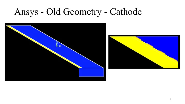
Ansys - Old Geometry - Cathode
1
Ansys - Old Geometry - Cathode 1 Ansys - New Geometry - Cathode - - PowerPoint PPT Presentation
Ansys - Old Geometry - Cathode 1 Ansys - New Geometry - Cathode lamella (PCB and copper strips) geometry is closer to realitiy additional gas volumes 2 Ansys - New Geometry - GEM unit cell Kapton layer with gas holes complete
1
2
3
corrected gap size compared to geometry showed before
4
5
6
17.4
7
16.4
8
20.4
new geometry without GEM
9
20.4
new geometry without GEM
10
21.4
new geometry without GEM
11
install new Ansys Simulation and get it to work get GEM geometry to work (convergence problem) add voltage at bottom of induction area material properties take closer look at Garfield++ simulation (distribution of detected electrons, influence of GEM, correlation of y- position of created electrons and detected charge?, ...)
12
12.5
13
12.5
14
13.5
15
13.5
16
new geometry without GEM (ansys2020)
12.5
18
partial GEM complete GEM
12.5/13.5
19
12.5/13.5
20
12.5/13.5
21
→ same voltage → 1 mm more at the right compared to previous geometry → but different potential distribuation
12.5/13.5
22
08.5
23
14.5
24
14.5
25
20.5
26
∆U(GEMO_GEMU)=300V, ∆U(GEMU_bottom)=100V and electric field vectors
19.5
27
20.5
28
diffx = 90V, diffy = 400V, ∆U(cathode_GEMO)=100V, ∆U(GEMO_GEMU)=300V, ∆U(GEMU_bottom)=100V → no electrons can be detected ↯
20.5
29
diffx = 90V, diffy = 400V, ∆U(cathode_GEMO)=100V, ∆U(GEMO_GEMU)=300V, ∆U(GEMU_bottom)=100V → seems like electric field in GEM is not homogenous ?↯