A multiplexer implementation Sum of products form: i 1 .c + i 0 .c - - PowerPoint PPT Presentation

a multiplexer implementation
SMART_READER_LITE
LIVE PREVIEW

A multiplexer implementation Sum of products form: i 1 .c + i 0 .c - - PowerPoint PPT Presentation

Lecture 7: Logic design Binary digital logic circuits: Two voltage levels (ground and supply voltage) for 0 and 1 Built from transistors used as on/off switches Analog circuits not very suitable for generic computing Digital


slide-1
SLIDE 1

Inf2C Computer Systems - 2012-2013 1

Lecture 7: Logic design

§ Binary digital logic circuits:

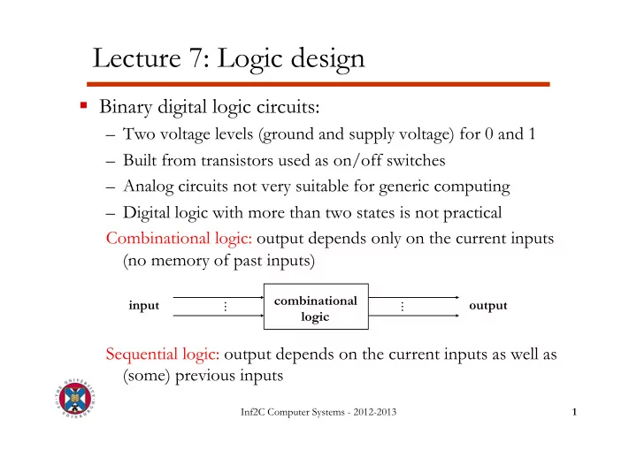
– Two voltage levels (ground and supply voltage) for 0 and 1 – Built from transistors used as on/off switches – Analog circuits not very suitable for generic computing – Digital logic with more than two states is not practical Combinational logic: output depends only on the current inputs (no memory of past inputs)

combinational logic

. . . . . .

input

  • utput

Sequential logic: output depends on the current inputs as well as (some) previous inputs

slide-2
SLIDE 2

Inf2C Computer Systems - 2012-2013 2

Combinational logic circuits

§ Inverter (or NOT gate): 1 input and 1 output

“invert the input signal”

§ AND gate: minimum 2 inputs and 1 output

“output 1 only if both inputs are 1” input

  • utput

IN OUT OUT = IN IN1 IN2 OUT IN1 IN2 OUT OUT = IN1 . IN2 1 1 1 1 1 1 1

slide-3
SLIDE 3

Inf2C Computer Systems - 2012-2013 3

Combinational logic circuits

§ OR gate:

– “output 1 if at least one input is 1”

§ NAND gate:

– “output 1 if both inputs are not 1” (NOT AND)

IN1 IN2 OUT IN1 IN2 OUT OUT = IN1 + IN2 1 1 1 1 1 1 1 IN1 IN2 OUT IN1 IN2 OUT OUT = IN1 . IN2 1 1 1 1 1 1 1

slide-4
SLIDE 4

Inf2C Computer Systems - 2012-2013 4

Combinational logic circuits

§ NOR gate:

“output 1 if no input is 1” (NOT OR)

§ Multiple-input gates:

IN1 IN2 IN1 IN2 OUT OUT = IN1 + IN2 1 1 1 1 1 OUT IN1 INn OUT

. . .

OUT = 1 if all INi=1

IN1 INn OUT

. . .

OUT = 1 if any INi=1

AND OR

slide-5
SLIDE 5

Inf2C Computer Systems - 2012-2013 5

Multiplexer

§ Multiplexer: a circuit for selecting one of many inputs

z = i0 i1 z c i0, if c=0 i1, if c=1 i0 i1 c z 1 1 1 1 1 1 1 1 1 1 1 1 1 1 1 1

z = i0.i1.c + i0.i1.c + i0.i1.c + i0.i1.c = i0.i1.c + i0.i1.c + i0.i1.c + i0.i1.c = (i0 + i0).i1.c + i0.(i1 + i1).c = i1.c + i0.c

“sum of products form”

slide-6
SLIDE 6

Inf2C Computer Systems - 2012-2013 6

A multiplexer implementation

§ Sum of products form:

– Can be implemented with 1 inverter, 2 AND gates and 1 OR gate: i1.c + i0.c

i0 z c i1

§ Sum of products is not practical for circuits with large number of inputs (n)

– The number of possible products can be proportional to 2n

slide-7
SLIDE 7

Inf2C Computer Systems - 2012-2013 7

Arithmetic circuits

§ 32-bit adder § Full adder:

a0

. . .

. . . . . .

b0 a31 b31 s32 s0

64 inputs → too complex for sum of products

a b sum carry(-out) c (carry-in)

a b c carry sum 1 1 1 1 1 1 1 1 1 1 1 1 1 1 1 1 1 1 1 1

sum = a.b.c + a.b.c + a.b.c + a.b.c carry = b.c + a.c + a.b

slide-8
SLIDE 8

Inf2C Computer Systems - 2012-2013 8

Ripple carry adder

§ 32-bit adder: chain of 32 full adders

– Carry bits ci are computed in sequence c1, c2, … , c32 (where c32 = s32), as ci depends on ci-1 – Since sum bits si also depend on ci, they too are computed in sequence

. . .

c0 b0 a0 s0 c1 b1 a1 s1 c31 b31 a31 s31 s32

1 bit full-adder

slide-9
SLIDE 9

Inf2C Computer Systems - 2012-2013 9

Propagation Delays

§ Propagation delay = time delay between input signal change and output signal change at the other end § Delay depends on technology (transistor, wire capacitance, etc.) and number of gates driven by the gate’s output (fan out) § e.g.: Sum of products circuits: 3 2-input gate delays (inverter, AND, OR) → very fast! § e.g.: 32-bit ripple carry adder: 65 2-input gate delays (1 AND + 1 OR for each of 31 carries to propagate; 1 inverter + 1 AND + 1 OR for S31) → slow

slide-10
SLIDE 10

Inf2C Computer Systems - 2012-2013 10

Sequential logic circuits

§ Output depends on current inputs as well as past inputs

– The circuit has memory

§ Sequences of inputs generate sequences of

  • utputs ⇒ sequential logic

combinational logic

. . . . . . . . . . . . . . .

input

  • utput

feedback sequential logic

slide-11
SLIDE 11

Inf2C Computer Systems - 2012-2013 11

Sequential logic circuits

§ For a fixed input and n feedback signals, the circuit can have up to 2n stable states

– E.g. n=1 → one state if feedback signal = 0

  • ne state if feedback signal = 1

§ Example: SR latch

– Inputs: R, S – Feedback: q, q – Output: Q

S R Q Q q q

slide-12
SLIDE 12

Inf2C Computer Systems - 2012-2013 12

SR Latch

S R Q Q q q 1 1 1 1 1 1 q q

§ Truth table: § Usage: 1-bit memory

– Keep the value in memory by maintaining S=0 and R=0 – Set the value in memory to 0 (or 1) by setting R=1 (or S=1) for a short time

S R Qi u=unused 1 1 1 1 Qi-1 1 u S R Q=1 S R Q=0

slide-13
SLIDE 13

Inf2C Computer Systems - 2012-2013 13

Timing of events

§ Asynchronous sequential logic

– State (and possibly output) of circuit changes whenever inputs change

§ Synchronous sequential logic

– State (and possibly output) can only change at times synchronized to an external signal → the clock

input

  • utput

input

  • utput

clock

slide-14
SLIDE 14

Inf2C Computer Systems - 2012-2013 14

D flip-flop

§ Edge-triggered flip-flop: on a +ve clock edge, D is copied to Q § Can be used to build registers:

D Q clock D Q input clock

  • utput

D3 Q3 D2 Q2 D1 Q1 D0 Q0 clock D3 D2 D1 D0 Q3 Q2 Q1 Q0 clock

4-bit register

slide-15
SLIDE 15

Inf2C Computer Systems - 2012-2013 15

General sequential logic circuit

§ Operation:

– At every rising clock edge next state signals are propagated to current state signals – Current state signals plus inputs work through combinational logic and generate output and next state signals

combinational logic

. . . . . . . . . . . .

input

  • utput

Next state signals

Q0 Dm D0 Qm

Current state signals

clock

. . . . . .

slide-16
SLIDE 16

Inf2C Computer Systems - 2012-2013 16

Hardware FSM

§ A sequential circuit is a (deterministic) Finite State Machine – FSM § Example: Vending machine

– Accepts 10p, 20p coins, sells one product costing 30p, no change given – Coin reader has 2 outputs: a,b for 10p, 20p coins respectively – Output z asserted when 30p

  • r more has been paid in
slide-17
SLIDE 17

Inf2C Computer Systems - 2012-2013 17

FSM implementation

§ Methodology:

– Choose encoding for states, e.g S0=00, …, S3=11 – Build truth table for the next state s1', s0' and output z – Generate logic equations for s1', s0', z – Design comb logic from logic equations and add state- holding register

s1 s0 a b s1' s0' z 1 1 1 1 1 1 1 1 1 1 1 1 1 comb. logic a z

S1 S0' S1' S0 clk

b