
SLIDE 1
Chapter 5: Selectors and Shifters
Computer Structure - Spring 2004
- Dr. Guy Even
Tel-Aviv Univ.
– p.1
Goals
Selectors: review definition of multiplexer. build (n : 1)-multiplexers. Shifters: Cyclic shifter (Barrel shifter) Logical Shifter Arithmetic Shifter
– p.2
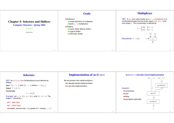
Multiplexer
DEF: A MUX-gate (also known as a (2 : 1)-multiplexer) is a combinational gate that has three inputs D[0], D[1], S and
- ne output Y . The functionality is defined by
Y =
- D[0]
if S = 0 D[1] if S = 1. Equivalently: Y = D[S]
mux 1 D[0] D[1] S Y
– p.3
Selectors
DEF: An (n:1)-MUX is a combinational circuit defined as follows:
Input: D[n − 1 : 0] and S[k − 1 : 0] where k = ⌈log2 n⌉. Output: Y ∈ {0, 1}. Functionality:
Y = D[ S]. Example: Let n = 4, D[3 : 0] = 0101, and S[1 : 0] = 11. The
- utput Y should be 1.
- D - data input
- S - select input
simplify: assume that n is a power of 2, namely, n = 2k.
– p.4
Implementation of (n:1)-MUX
We will present two implementations: a decoder based implementation a tree-like implementation
– p.5
(n:1)-MUX : a decoder based implementation
Question: correctness cost delay asymptotic optimality
k 2k 2k 2k 1
DECODER(k)
S[k − 1 : 0] D[n − 1 : 0] Y
AND(2k) OR-tree(2k)
– p.6