3D slim edge silicon sensors: Processing, Yield and QA Cinzia Da Vi - - PowerPoint PPT Presentation

3d slim edge silicon sensors
SMART_READER_LITE
LIVE PREVIEW

3D slim edge silicon sensors: Processing, Yield and QA Cinzia Da Vi - - PowerPoint PPT Presentation

3D slim edge silicon sensors: Processing, Yield and QA Cinzia Da Vi , Uni. Manchester. HSTD-8 Taipei 5 th December 2011 for the ATLAS IBL production Cinzia Da Vi, The University of Manchester, UK GF Dalla Betta (Trento University), G.


slide-1
SLIDE 1

Cinzia Da Viá , Uni. Manchester. HSTD-8 Taipei 5th December 2011

3D slim edge silicon sensors: Processing, Yield and QA for the ATLAS IBL production

Cinzia Da Vià, The University of Manchester, UK

GF Dalla Betta (Trento University), G. Pellegrini, C. Fleta (CNM Barcelona)

  • M. Boscardin , G. Giacomini, N. Zorzi(FBK Trento)A. Kok, T-E Hansen (SINTEF),
  • J. Hasi, C. Kenney (SLAC), S, Parker (Hawaii). S. Grinstein (IFAE), A. Micelli

(Udine), C. Gemme, G. Darbo (Genova) D-L Pohl (Bonn).

Introduction 3D silicon for the ATLAS IBL Quality Assurance Production Yield Summary and outlook

CNM

slide-2
SLIDE 2

Cinzia Da Viá , Uni. Manchester. HSTD-8 Taipei 5th December 2011

Introduction

  • The Large Hadron Collider will have its first upgrade in 2013-14 to

reach its nominal energy of 14TeV in the center of mass

  • ATLAS will use the LHC Upgrade time to insert an extra pixel layer

33mm from the beam. For this to be possible the current beam pipe will be replaced with a smaller diameter one (More on this from S. Grisnstein on Tuesday)

  • Diamond, 3D and new planar silicon sensors with slim edges were

competing as sensor technologies for the IBL

  • After one year of intense qualification work and looking at all risks

involved a review panel recommended to load the IBL with 75% planar and 25% 3D silicon sensors

  • Diamond will be used to build a beam condition monitor in the IBL

region (see A. Gorisek)

  • More on 3D sensors from G. Pellegrini and M. Povoli and some details
  • n the common IBL 2011 test beams results from I. Rubinskiy
slide-3
SLIDE 3

Cinzia Da Viá , Uni. Manchester. HSTD-8 Taipei 5th December 2011

ATLAS IBL Layout and parameters

Layout – 14 Staves – 14 FE chips/stave – For 3D single chips (224 to build 25%) – For planar double chips (448 to build 75%) These numbers have a redundancy

  • f 100% to account for loading

yield Requirements – “Hermetic” to straight tracks in Φ (1.8º overlap) – No overlap in Z: minimize gap between sensor active area. Parameters – IBL envelope: 9 mm in R – <R> = 33 mm. – Z = 60 cm (active length). – η = 2.5 coverage.

slide-4
SLIDE 4

Cinzia Da Viá , Uni. Manchester. HSTD-8 Taipei 5th December 2011

IBL sensors specifications FE-I4

FE-I3 FE-I4 Pixel Size [μm2] 50×400 50×250 Pixel Array 18×160 80×336 Chip Size [mm2] 7.6×10.8 20.2×19.0 Active Fraction 74 % 89 % Analog Current [μA/pix] 26 10 Digital Current [μA/pix] 17 10 Analog Voltage [V] 1.6 1.4 Digital Voltage [V] 2 1.2 pseudo-LVDS out [Mb/s] 40 160

Preamp Amp2 FDAC TDAC Config Logic discri 50 mm

250 mm

synthezised digital region (1/4th )

160 18

FE-I3

FE-I4A-B

slide-5
SLIDE 5

Cinzia Da Viá , Uni. Manchester. HSTD-8 Taipei 5th December 2011

3D detectors

DEPLETION VOLTAGES < 10 V 70 V After irradiation 180 V 1000V Power dissipation goes with V goes with V EDGE SENSITIVITY < 5 mm 500 mm CHARGE 1 MIP (300 mm) 24000e- 24000e- CAPA CITANCE 30-50f ~20fF COLLECTION DISTANCE 50 mm 300 mm SPEED 1-2ns 10-20 ns

3D 3D planar nar

Drif ift t lines s parall rallel l to the surf rface ce MEDICI DICI simulatio mulation

  • f a 3

3D struc ructure

p+ n+

  • -

+ + + +

  • +

PLANAR ~ 0.2-1mm guard rings particle 300 mm n+ p+ 50 mm

  • -

+

  • +

+

  • 3D

n+ Active edge 50 mm

  • particle

300 mm

3D has Lower charge sharing probability

n

e i diffusion

slide-6
SLIDE 6

Cinzia Da Viá , Uni. Manchester. HSTD-8 Taipei 5th December 2011

3D sensors for IBL

  • 3D is a silicon sensor technology

designed specifically to be radiation hard

  • The current design parameters have

been tuned to

  • ptimize

the IBL constraints in terms of signal amplitude, noise, bias voltage and consequent system requirements

  • First prototypes were available at the

end of 1990ties. Few years later more industries started producing 3D sensors

  • In June 2009, four facilities decided

to „join‟ knowhow and effort for a common goal: optimise the process and speedup a parallel industrialization strategy to guarantee a reliable production of 3D sensors. Two were finally selected for the „fast track‟ ATLAS IBL. The remaining two still contribute to the effort and looking into future optimizations of the design

Common

  • n floor-plan

lan wafer r layou

  • ut

3

slide-7
SLIDE 7

Cinzia Da Viá , Uni. Manchester. HSTD-8 Taipei 5th December 2011

Original Strategy: qualify both full3D and DSDC with Common Floor-Plan Design

8 8 x FE-I4 I4

  • 9

9 x FE-I3 I3

  • Other

er test t structures tures

Design by GF Dalla Betta, C. Kenney, A. Kok, G Pellegrini

  • 15.0
  • 13.0
  • 11.0
  • 9.0
  • 7.0
  • 5.0
  • 3.0
  • 1.0 0

10 20 30 40 50 60 70 80 Leakage Current (µA) Bias Voltage (V) FE-I4 1 FE-I4 2 FE-I4 3 FE-I4 4 FE-I4 5 FE-I4 6 FE-I4 7 FE-I4 8

FE-I4 full 3D with Active Edges wafer Fabricated at SINTEF With holes filled At Stanford

J Hasi, C. Kenney,

  • A. Kok, T-E Hansen
slide-8
SLIDE 8

Cinzia Da Viá , Uni. Manchester. HSTD-8 Taipei 5th December 2011

8

QA action Level Description/Comments

Visual inspection Each fabrication step Check for shorts, discoloration or anomalies

  • n the sensor surface, front –back

misalignment Wafer bow completed wafer Measurement of wafer bow, no problem for bump-bonding but potential risk of higher leakage and electrodes misalignment Critical steps analysis with test wafers DRIE Poly-doping Optical inspection, test of resistance, presence of voids or anomalies IV on test structures Completed wafer Gives a global indication of wafer

  • quality. Test structures are distributed

all around the wafer perimeter where IV would indicate worst case. IV on FE-I4 sensors Used by CNM On wafer and after UBM Useful to select good sensors after process completion and after UBM

  • deposition. Requires a guard ring

Use of temporary metal Used by FBK On wafer Gives a reliable measurement of the sensor quality at pixel level, performed before final metal deposition. X-Ray inspection at IZM After UBM After bump-bonding Performed at IZM

Each wafer should have at least 3 good FE-I4 3D sensors to be selected.

QA and Sensor selection criteria

slide-9
SLIDE 9

Cinzia Da Viá , Uni. Manchester. HSTD-8 Taipei 5th December 2011

9

3D sensors Selection Parameters

The following specifications are required to qualify a 3D device as functioning correctly before bump-bonding:

  • Operation at room temperature (20−24 oC)
  • Vdepl ≤ 15V
  • Vop ≥ Vdepl +10V where Vdepl is the full depletion voltage.
  • Current at 20 − 24 oC at operation voltage: I (Vop) < 2μA per sensor
  • For GR measurement (CNM): IGR (Vop) < 200nA per sensor
  • Breakdown voltage: Vbd > 25V
  • Slope: [I(Vop)/I(Vop-5V)] < 2

I-V measurements are performed on each sensor on wafer with a probe station by the manufacturer using either a temporary metal or by probing the guard ring current

FBK temporary metal CNM guard ring current

slide-10
SLIDE 10

Cinzia Da Viá , Uni. Manchester. HSTD-8 Taipei 5th December 2011

0.01 0.1 1 10 100

50 100 150 200 I(uA) V(V)

Wafer 17 GR current on wafer vs total current after bonding, 20ºC

17-4-chip 17-4-wafer 17-1-chip 17-1-wafer 17-2-chip 17-2-wafer 17-3-chip 17-3-wafer '17-7-chip '17-7-wafer

CNM IBL Qualification wafers before and after bump-bonding

GR current identifies potential defects Also could be enhanced by stress and neighbour sensors 100% Reproduced behaviour before and after BB

  • C. Fleta. S. Grinstein, G. Pellegrini

0.01 0.1 1 10 100 50 100 150 200

I(uA) V(V)

Wafer 15 GR current on wafer vs total current after bonding, 20ºC

15-4-chip 15-4-wafer 15-1-chip 15-1-wafer 15-5-chip 15-5-wafer 15-2-chip 15-2-wafer

0.01 0.1 1 10 100 50 100 150 200

I(uA) V(V)

Wafer 12 GR current on wafer vs total current after bonding, 20ºC

12-4-chip 12-4-wafer 12-1-chip 12-1-wafer 12-8-chip 12-8-wafer 12-6-chip 12-6-wafer

W17 6/8 W16 4/8 W12 4/8 10 25

slide-11
SLIDE 11

Cinzia Da Viá , Uni. Manchester. HSTD-8 Taipei 5th December 2011

Compilation qualification CNM assemblies after BB

I< 2mA Vop ≥ Vdepl +10V (20V) Vbd > 25V Slope: [I(Vop)/I(Vop-5V)] < 2

slide-12
SLIDE 12

Cinzia Da Viá , Uni. Manchester. HSTD-8 Taipei 5th December 2011

3D IBL production: technical sheet for each

  • f the selected wafers: ex. CNM

bowing 7

slide-13
SLIDE 13

Cinzia Da Viá , Uni. Manchester. HSTD-8 Taipei 5th December 2011

13

Yield production run : CNM 1

G Pellegrini, C. Fleta 4 5 8 6 3(+2) 6 5 5

WAFERS sent for bump-bonding Yield on selected wafers 42/64=66%

slide-14
SLIDE 14

Cinzia Da Viá , Uni. Manchester. HSTD-8 Taipei 5th December 2011

Selection Criteria and QA - FBK

slide-15
SLIDE 15

Cinzia Da Viá , Uni. Manchester. HSTD-8 Taipei 5th December 2011

1E+01 1E+02 1E+03 1E+04 1E+05 1E+06 10 20 30 40 50 60 70 80

I [nA] V_rev [V] FEI4 sensors - total current

S1 S2 S3 S4 S5 S6 S7 S8 #6 #5

FBK ATLAS09 Wafer 14 : selected for bump-bonding

  • Temporary metal shorts together a

full column of pixel.

  • All columns IV measured separately

and summed up together.

  • Metal etched off before being sent

for bump-bonding

  • N. Zorzi, G. Giacomini
slide-16
SLIDE 16

Cinzia Da Viá , Uni. Manchester. HSTD-8 Taipei 5th December 2011

ATLAS09 Wafer 14 before and after bump-bonding

  • N. Zorzi, G. Giacomini, D-L. Pohl, G. Darbo

1E+00 1E+01 1E+02 1E+03 1E+04 1E+05 1E+06 10 20 30 40 50 60 70 80 I [nA] V_rev [V]

SCC111

  • W14

Assy S7

  • IV

before/a er bump-bonding

On Wafer A er Flip-chip 1E+00 1E+01 1E+02 1E+03 1E+04 1E+05 1E+06 10 20 30 40 50 60 70 80 I [nA] V_rev [V]

SCC112

  • W14

Assy S3

  • IV

before/a er bump bonding

On Wafer A er Flip-chip 1E+00 1E+01 1E+02 1E+03 1E+04 1E+05 1E+06 10 20 30 40 50 60 70 80 I [nA] V_rev [V]

SCC113

  • W14

Assy S4

  • IV

before/a er bump-bonding

On Wafer A er Flip-chip 1E+00 1E+01 1E+02 1E+03 1E+04 1E+05 1E+06 10 20 30 40 50 60 70 80 I [nA] V_rev [V]

SCC114

  • W14

Assy S5

  • IV

before/a er bump-bonding

On Wafer A er Flip-chip

Disconnected bumps

slide-17
SLIDE 17

Cinzia Da Viá , Uni. Manchester. HSTD-8 Taipei 5th December 2011

Compilation FBK assemblies after BB

I < 2mA Vop ≥ Vdepl +10V (20V) Vbd > 25V Slope: [I(Vop)/I(Vop-5V)] < 2

  • A. Micelli , C. Gemme
slide-18
SLIDE 18

Cinzia Da Viá , Uni. Manchester. HSTD-8 Taipei 5th December 2011

1E+01 1E+02 1E+03 1E+04 1E+05 1E+06 10 20 30 40 50 60 70 80 I [nA] V_rev [V]

FEI4 sensors

  • total

current

  • S1

S2 S3 S4 S5 S6 S7 S8 1E+01 1E+02 1E+03 1E+04 1E+05 1E+06 10 20 30 40 50 60 70 80 I [nA] V_rev [V]

FEI4 sensors

  • total

current

  • S1

S2 S3 S4 S5 S6 S7 S8 1E+01 1E+02 1E+03 1E+04 1E+05 1E+06 10 20 30 40 50 60 70 80 I [nA] V_rev [V]

FEI4 sensors

  • total

current

  • S1

S2 S3 S4 S5 S6 S7 S8 1E+01 1E+02 1E+03 1E+04 1E+05 1E+06 10 20 30 40 50 60 70 80 I [nA] V_rev [V]

FEI4 sensors

  • total

current

  • S1

S2 S3 S4 S5 S6 S7 S8 1E+01 1E+02 1E+03 1E+04 1E+05 1E+06 10 20 30 40 50 60 70 80 I [nA] V_rev [V]

FEI4 sensors

  • total

current

  • S1

S2 S3 S4 S5 S6 S7 S8 1E+01 1E+02 1E+03 1E+04 1E+05 1E+06 10 20 30 40 50 60 70 80 I [nA] V_rev [V]

FEI4 sensors

  • total

current

  • S1

S2 S3 S4 S5 S6 S7 S8

Yield production run : FBK ATLAS10

  • N. Zorzi, G. Giacomini

Run Completed in July 2011 Yield on selected wafers: 29/48 = 60%

slide-19
SLIDE 19

Cinzia Da Viá , Uni. Manchester. HSTD-8 Taipei 5th December 2011

19 W18 5 W20 4 W22 5 W23 4 W25 4

Yield production run : FBK ATLAS10

  • N. Zorzi, G. Giacomini

Completed in September 2011 Yield on selected wafers: 22/40 = 55% Total Yield selected A10 FBK = 57.5% total good sensors =51

slide-20
SLIDE 20

Cinzia Da Viá , Uni. Manchester. HSTD-8 Taipei 5th December 2011

20

  • A10 completed and tested. 22 wafers measured 12 selected for bump-bonding
  • CNM1 completed on schedule the first fabrication batch. 18 selected for bump-

bonding CNM2 12 wafers completed and being tested, the remaining by Jan 2012

Batch Status Compl. Date tested Selected wafers Yield on selected Number

  • f good

sensors A10

Completed July/sept11 20 12 56% 54

A11

Completed 18-31Oct 11

  • A12

Ongoing 30 Jan12

  • CNM1

Completed 10-31Oct 19 18 60% 86

CNM2

Ongoing 30Dec 15

  • CNM3

Ongoing 30Jan

  • TOTAL=

Today 30 58% 140 TO IZM

11-11-11

30 58% 140

IBL 3D Processing status Summary

12

slide-21
SLIDE 21

Cinzia Da Viá , Uni. Manchester. HSTD-8 Taipei 5th December 2011

21

Summary

The 3DATLAS collaboration committed to produce 224 3D sensors compatible with the ~4cm 2 FE-I4 at CNM and FBK by IBL loading time in spring 2012

  • 20+22 production wafers have been completed, 39 tested,
  • 30 selected for IZM batch with a total yield of ~58%
  • = 140 class A sensors are ready and waiting to be bump-bonded

Further batches are in an advanced processing state both at CNM and FBK To be completed by December 2011 and January 2012

  • Highlights:
  • Efficiency of CNM assemblies irradiated at 5x10^15 n/cm2 measured after

bias (160V) and lowered threshold (1200-1500e) at 15degrees=98.9% and resolution 9.2um for cluster size2

  • Reliable operation after 5x10¹⁵ncm-2 at -5oC during test beam
  • Edge efficiency for slim fences double sided 3D measured at ~150 um from

physical edge in test beams after irradiation (see I. Rubinskiy talk)

slide-22
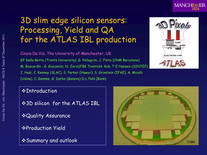
SLIDE 22

Cinzia Da Viá , Uni. Manchester. HSTD-8 Taipei 5th December 2011

22

3D ATLAS R&D Collaboration

  • B. Stugu, H. Sandaker, K. Helle, (Bergen University), M. Backhaus, M. Barbero, J.

Janssen, F. Hügging, M. Karagounis, V. Kostyukhin, H. Krüger, D-L Pohl, J-W Tsung, N. Wermes (Bonn University), M. Capua; S. Fazio, A. Mastroberardino; R. Mendicino, G. Susinno (Calabria University), C. Gallrapp, B. Di Girolamo; D. Dobos, A. La Rosa, H. Pernegger, S. Roe (CERN), T. Slavicek, S. Pospisil (Czech Technical University), K. Jakobs,

  • M. Köhler, U. Parzefall (Freiburg University), G. Darbo, G. Gariano, C. Gemme, A. Rovani,
  • E. Ruscino (University and INFN of Genova), C. Butter, R. Bates, V. Oshea (Glasgow

University), S. Parker (The University of Hawaii), M. Cavalli-Sforza, S. Grinstein, I. Korokolov, K. Shota Tsiskaridze C. Padilla (IFAE Barcelona), K. Einsweiler, M. Garcia- Sciveres (Lawrence Berkeley National Laboratory), M. Borri, C. Da Vià, J. Freestone, C. Lai, C. Nellist, J. Pater, R. Thompson, S.J. Watts (The University of Manchester), M. Hoeferkamp, S. Seidel (The University of New Mexico), E. Bolle, H. Gjersdal, K-N Sjoebaek, S. Stapnes, O. Rohne, (Oslo University) D. Su, C. Young, P. Hansson, P. Grenier, J. Hasi, C. Kenney, M. Kocian, P. Jackson, D. Silverstein (SLAC), H. Davetak, B. DeWilde, D. Tsybychev (Stony Brook University). G-F Dalla Betta, M. Povoli (University and INFN of Trento), M. Cobal, M-P Giordani, L. Selmi, A. Cristofoli, D. Esseni, A. Micelli,

  • P. Palestri (University of Udine)

Processing Facilities: C. Fleta, M. Lozano G. Pellegrini, D.Quirion (CNM Barcelona, Spain); (M. Boscardin, A. Bagolini, G. Giacomini, F. Mattedi, C. Piemonte, S. Ronchin, E. Vianello,

  • N. Zorzi (FBK-Trento, Italy) , T-E. Hansen, T. Hansen, A. Kok, N. Lietaer ( SINTEF

Norway), J. Hasi, C. Kenney (Stanford). J. Kalliopuska, A. Oja (VTT , Finland)* 18 institutions and 5 processing facilities

22 Formed in 2007 to industrialise 3D technology for ATLAS pixel upgrades

slide-23
SLIDE 23

Cinzia Da Viá , Uni. Manchester. HSTD-8 Taipei 5th December 2011

spares

slide-24
SLIDE 24

Cinzia Da Viá , Uni. Manchester. HSTD-8 Taipei 5th December 2011

Simulations (from A. Zoboli PhD thesis, Trento, March 2009)

  • D. Pennicard, Glasgow IEEE/NSS 08

Simulations and data shows that The response of full 3D and 3D-DDTC is very close if the electrode penetration stops 25 mm from the surface Before and after irradiation

Consistent performance of the considered 3D designs

slide-25
SLIDE 25

Cinzia Da Viá , Uni. Manchester. HSTD-8 Taipei 5th December 2011

QA for wafer bowing is < 60 microns with an alignment <5 microns This is valid for both FBK (this slide) and CNM from E. Vianello, FBK, 3D processing meeting 19-5-11

25

slide-26
SLIDE 26

Cinzia Da Viá , Uni. Manchester. HSTD-8 Taipei 5th December 2011

20 40 60 80 100 120 140 160 1 10

15

2 10

15

3 10

15

4 10

15

5 10

15

6 10

15

CNM Voltage FBK voltage

Operational Voltage [V] Fluence [ncm

  • 2]

Leakage currents and operational voltages After irradiation

T [oC] FEC-off Fluence x 10 15 [ncm-2] Vop [V] Current [uA] Per chip

  • 20 CNM

2 5 6 63 151 151 67 149 188

  • 15 CNM

2 5 6 63 152 117 275 326

  • 15 FBK

2 5 60 140 137 340

  • 10 CNM

2 5 64 158 203 466

  • 5 CNM

2 5 63 145 569 795

  • A. Micelli, C. Gemme, S. Grinstein

100 200 300 400 500 1 10

15

2 10

15

3 10

15

4 10

15

5 10

15

6 10

15

7 10

15

CNM T=-15

  • C

CNM T=-10 oC CNM T= -20

  • C

FBK T= -15

  • C

Leakage current [uA] Fluence [ncm

  • 2
CNM

Confirms higher damage for second raw samples during last KA proton irradiation

CNM SSC97

Fluence [ncm-2] Fluence [ncm-2]

slide-27
SLIDE 27

Cinzia Da Viá , Uni. Manchester. HSTD-8 Taipei 5th December 2011

Power dissipation at different Temperatures after irradiation

Temp . [oC] Fluence x1015 [ncm-2] W CNM [mWcm-2] W FBK mWcm-2]

  • 20

2 5 6 1.1 5.7 7.1

  • 15

2 5 6 1.9 10.5 12.7 2.5 13

  • 10

2 5 3.3 17.3

  • 5

2 5 5 29

0.1 1 10 100 1 10

15 2 10 15 3 10 15 4 10 15 5 10 15 6 10 15 7 10 15 8 10 15

CNM T=-15

  • C

CNM T=-10

  • C

CNM T=-20

  • C

CNM T=-5

  • C

FBK T=-15

  • C

Power dissipation [mWcm

  • 2]

Fluence [ncm

  • 2]

IBL requirement on sensor Power dissipation < 200 mW/cm2 at 5 x 10¹⁵ neq/cm2 and -15 o C (after annealing)

  • C. Gemme, A. Micelli, S. Grinstein
slide-28
SLIDE 28

Cinzia Da Viá , Uni. Manchester. HSTD-8 Taipei 5th December 2011 5000 10000 15000 20000 1 1015 2 1015 3 1015 4 1015 5 1015 6 1015 Most Probable Value [e-] Fuence [ncm-2]

Most probable signal after IBL fluence

Compilation of Stanford, CNM,FBK

20 40 60 80 100 2 1015 4 1015 6 1015 8 1015 1 1016

CNM/Glasgow [ D. Pennicard, IEEE/NSS 2008] FBK-annealed [A. Zoboli PhD Thesis, 2009] STA [ NIMA 604 (2009) 505-511

Signal Efficiency [%] Fluence [ncm-2]

PRELIMINARY

  • C. Da Via June 09

MPS predicted=230mm x 75e- = 17 250 e-

Fluence [ncm-2] MPS [e-] 17250 1x10¹⁵ 16380 5x10¹⁵ 12075

slide-29
SLIDE 29

Cinzia Da Viá , Uni. Manchester. HSTD-8 Taipei 5th December 2011

200 mm guard fences

Design and simulation GF Dalla Betta, M. Povoli Trento Cut line pixel Junction Column Ohmic Column Active area (corner pixel) pixel

z

200 mm

3D-CNM34, irradiated with protons at 5E15neq/cm2: 1D hit efficiency in the long pixel direction for edge

  • pixels. All edge pixels have been added together.

Operation conditions are: FE-I4 threshold = 1300e, bias voltage = -140V, magnetic field = 1.6T, tilt angle = 0 degrees.​ Edge pixel: regular length 250 mm

  • Effective inactive area from

dicing: ~200μm.

  • Actual efficiency extends nominal

inactive length: 50%: 20-30μm

  • Same for all 3D samples.

Z

Analysis IFAE Barcelona More data from

  • I. Rubinskiy IBL

Test beam data

slide-30
SLIDE 30

Cinzia Da Viá , Uni. Manchester. HSTD-8 Taipei 5th December 2011

Guard Ring studies at CNM

41

  • S. Grinstein IFAE