
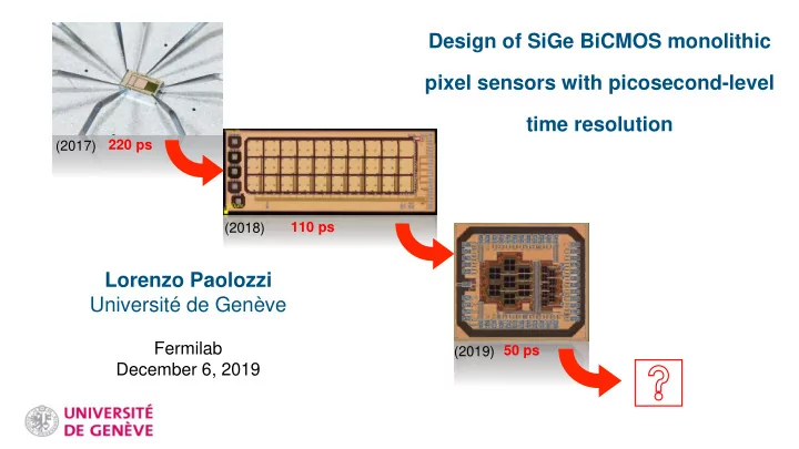
SLIDE 1
1
Lorenzo Paolozzi Université de Genève
Fermilab December 6, 2019
Design of SiGe BiCMOS monolithic pixel sensors with picosecond-level time resolution
(2017) (2018) (2019) 220 ps 110 ps 50 ps
Universit de Genve Fermilab 50 ps (2019) December 6, 2019 1 - - PowerPoint PPT Presentation
Design of SiGe BiCMOS monolithic pixel sensors with picosecond-level time resolution 220 ps (2017) 110 ps (2018) Lorenzo Paolozzi Universit de Genve Fermilab 50 ps (2019) December 6, 2019 1 Back in 2014 G. Iacobucci, R.
1
Fermilab December 6, 2019
(2017) (2018) (2019) 220 ps 110 ps 50 ps
2 /58
Five years of (hard) R&D
for ultra-fast, low noise signal amplification in particle detectors.
06/12/2019 - Fermilab Lorenzo Paolozzi 2
3 /58
06/12/2019 - Fermilab Lorenzo Paolozzi
Advanced track reconstruction
Hartmut F-W Sadrozinski et al 2018 Rep. Prog. Phys. 81 026101 3
4 /58
06/12/2019 - Fermilab Lorenzo Paolozzi
With timing
Advanced track reconstruction
Hartmut F-W Sadrozinski et al 2018 Rep. Prog. Phys. 81 026101 3
5 /58
06/12/2019 - Fermilab Lorenzo Paolozzi
Pile-up suppression
Hartmut F-W Sadrozinski et al 2018 Rep. Prog. Phys. 81 026101 4
6 /58
06/12/2019 - Fermilab Lorenzo Paolozzi
Pile-up suppression
Hartmut F-W Sadrozinski et al 2018 Rep. Prog. Phys. 81 026101 4
7 /58
06/12/2019 - Fermilab Lorenzo Paolozzi
NA62 GigaTracKer: hybrid pixels 300x300 µm2 no internal gain 130 ps time resolution
5
8 /58
06/12/2019 - Fermilab Lorenzo Paolozzi
NA62 GigaTracKer: hybrid pixels 300x300 µm2 no internal gain 130 ps time resolution
Low Gain Avalanche Detectors: hybrid pads 1x1 mm2 internal gain (10-100) 30 ps time resolution
Resolution [ps] Gain
5
9 /58
06/12/2019 - Fermilab Lorenzo Paolozzi
NA62 GigaTracKer: hybrid pixels 300x300 µm2 no internal gain 130 ps time resolution
Low Gain Avalanche Detectors: hybrid pads 1x1 mm2 internal gain (10-100) 30 ps time resolution
Resolution [ps] Gain
Is timing performance of silicon fully exploited ? How far are we from producing a monolithic 4D sensor with small pixels ?
5
10 /58
06/12/2019 - Fermilab Lorenzo Paolozzi 6
11 /58
06/12/2019 - Fermilab Lorenzo Paolozzi
𝒊+ 𝒇−
𝐽𝑗𝑜𝑒 𝑊
𝑝𝑣𝑢
(Recommended reading
7
12 /58
06/12/2019 - Fermilab Lorenzo Paolozzi
Sensor optimization for time measurement means: sensor time response independent from the particle trajectory
GND
8
13 /58
06/12/2019 - Fermilab Lorenzo Paolozzi
Sensor optimization for time measurement means: sensor time response independent from the particle trajectory
GND
𝑗
Induced current for a parallel plate readout from Shockley-Ramo’s theorem:
8
14 /58
06/12/2019 - Fermilab Lorenzo Paolozzi
Sensor optimization for time measurement means: sensor time response independent from the particle trajectory
GND
𝑗
Induced current for a parallel plate readout from Shockley-Ramo’s theorem:
Desired features:
8
15 /58
06/12/2019 - Fermilab Lorenzo Paolozzi
Sensor optimization for time measurement means: sensor time response independent from the particle trajectory
GND
𝑗
Induced current for a parallel plate readout from Shockley-Ramo’s theorem:
Desired features:
Scalar, saturated Scalar, uniform
𝑗
8
16 /58
06/12/2019 - Fermilab Lorenzo Paolozzi
When large clusters are absorbed at the electrodes, their contribution is removed from the induced current. The statistical origin of this variability of Iind makes this effect irreducible in PN-junction sensors.
+HV GND
𝒇− 𝒊+
Ionizing particle
𝐽𝑗𝑜𝑒 ≅ 𝑤𝑒𝑠𝑗𝑔𝑢 1 𝐸
𝑗
𝑟𝑗
9
17 /58
06/12/2019 - Fermilab Lorenzo Paolozzi
Charge collection noise represents an intrinsic limit to the time resolution for a semiconductor PN-junction detector. ~30 ps reached by present LGAD sensors.
Resolution [ps] Gain
Lower contribution from sensors without internal gain
10
18 /58
06/12/2019 - Fermilab Lorenzo Paolozzi
Pulse time Threshold Time
𝜏𝑢 = 𝜏𝑊 𝑒𝑊 𝑒𝑢 ≅ 𝐹𝑂𝐷 𝐽𝑗𝑜𝑒
11
19 /58
06/12/2019 - Fermilab Lorenzo Paolozzi
Pulse time Threshold Time
Need an ultra-fast, low noise, low power-consumption electronics with fast rise time and small capacitance. Our solution:
High 𝑔
𝑢, single transistor preamplifier.
𝜏𝑢 = 𝜏𝑊 𝑒𝑊 𝑒𝑢 ≅ 𝐹𝑂𝐷 𝐽𝑗𝑜𝑒
11
20 /58
06/12/2019 - Fermilab Lorenzo Paolozzi
𝐹𝑂𝐷2 = 𝐵1 𝑏𝑋 𝜐𝑁 𝐷𝑒𝑓𝑢 + 𝐷𝑗𝑜 2 + 𝐵2 𝑚𝑜2 𝜌 𝑑 𝐷𝑒𝑓𝑢 + 𝐷𝑗𝑜 2 + 𝐵3 𝑐1 + 𝑐2 𝜐𝑁
12
21 /58
06/12/2019 - Fermilab Lorenzo Paolozzi
𝐹𝑂𝐷2 = 𝐵1 𝑏𝑋 𝜐𝑁 𝐷𝑒𝑓𝑢 + 𝐷𝑗𝑜 2 + 𝐵2 𝑚𝑜2 𝜌 𝑑 𝐷𝑒𝑓𝑢 + 𝐷𝑗𝑜 2 + 𝐵3 𝑐1 + 𝑐2 𝜐𝑁 𝝊𝑵 ~ 𝟐 𝒐𝒕
12
22 /58
06/12/2019 - Fermilab Lorenzo Paolozzi
𝐹𝑂𝐷2 = 𝐵1 𝑏𝑋 𝜐𝑁 𝐷𝑒𝑓𝑢 + 𝐷𝑗𝑜 2 + 𝐵2 𝑚𝑜2 𝜌 𝑑 𝐷𝑒𝑓𝑢 + 𝐷𝑗𝑜 2 + 𝐵3 𝑐1 + 𝑐2 𝜐𝑁 How do MOS-FET and BJT compare in terms of noise? 𝝊𝑵 ~ 𝟐 𝒐𝒕
12
23 /58
06/12/2019 - Fermilab Lorenzo Paolozzi
𝐹𝑂𝐷2 = 𝐵1 𝑏𝑋 𝜐𝑁 𝐷𝑒𝑓𝑢 + 𝐷𝑗𝑜 2 + 𝐵2 𝑚𝑜2 𝜌 𝑑 𝐷𝑒𝑓𝑢 + 𝐷𝑗𝑜 2 + 𝐵3 𝑐1 + 𝑐2 𝜐𝑁
13
CMOS based amplifier
24 /58
06/12/2019 - Fermilab Lorenzo Paolozzi
CMOS based amplifier
2𝑙𝑈 ℎ 𝑛 Large ൗ
1 𝑔 contribution
𝐹𝑂𝐷2 = 𝐵1 𝑏𝑋 𝜐𝑁 𝐷𝑒𝑓𝑢 + 𝐷𝑗𝑜 2 + 𝐵2 𝑚𝑜2 𝜌 𝑑 𝐷𝑒𝑓𝑢 + 𝐷𝑗𝑜 2 + 𝐵3 𝑐1 + 𝑐2 𝜐𝑁
13
25 /58
06/12/2019 - Fermilab Lorenzo Paolozzi
BJT based amplifier
𝐹𝑂𝐷2 = 𝐵1 𝑏𝑋 𝜐𝑁 𝐷𝑒𝑓𝑢 + 𝐷𝑗𝑜 2 + 𝐵2 𝑚𝑜2 𝜌 𝑑 𝐷𝑒𝑓𝑢 + 𝐷𝑗𝑜 2 + 𝐵3 𝑐1 + 𝑐2 𝜐𝑁
14
26 /58
06/12/2019 - Fermilab Lorenzo Paolozzi
BJT based amplifier
𝐹𝑂𝐷2 = 𝐵1 𝑏𝑋 𝜐𝑁 𝐷𝑒𝑓𝑢 + 𝐷𝑗𝑜 2 + 𝐵2 𝑚𝑜2 𝜌 𝑑 𝐷𝑒𝑓𝑢 + 𝐷𝑗𝑜 2 + 𝐵3 𝑐1 + 𝑐2 𝜐𝑁
14
27 /58
06/12/2019 - Fermilab Lorenzo Paolozzi
𝐹𝑂𝐷series noise ∝ 𝑙1 ⋅ 𝐷𝑢𝑝𝑢
2
𝛾 + 𝑙2 ⋅ 𝑆𝑐𝐷𝑢𝑝𝑢
2
BJT based amplifier
𝐹𝑂𝐷2 = 𝐵1 𝑏𝑋 𝜐𝑁 𝐷𝑒𝑓𝑢 + 𝐷𝑗𝑜 2 + 𝐵2 𝑚𝑜2 𝜌 𝑑 𝐷𝑒𝑓𝑢 + 𝐷𝑗𝑜 2 + 𝐵3 𝑐1 + 𝑐2 𝜐𝑁
14
28 /58
06/12/2019 - Fermilab Lorenzo Paolozzi
𝐹𝑂𝐷series noise ∝ 𝑙1 ⋅ 𝐷𝑢𝑝𝑢
2
𝛾 + 𝑙2 ⋅ 𝑆𝑐𝐷𝑢𝑝𝑢
2
BJT based amplifier
𝐹𝑂𝐷2 = 𝐵1 𝑏𝑋 𝜐𝑁 𝐷𝑒𝑓𝑢 + 𝐷𝑗𝑜 2 + 𝐵2 𝑚𝑜2 𝜌 𝑑 𝐷𝑒𝑓𝑢 + 𝐷𝑗𝑜 2 + 𝐵3 𝑐1 + 𝑐2 𝜐𝑁
14
29 /58
06/12/2019 - Fermilab Lorenzo Paolozzi
For a NPN BJT, the amplifier current gain β can be expressed as:
15
30 /58
06/12/2019 - Fermilab Lorenzo Paolozzi
For a NPN BJT, the amplifier current gain β can be expressed as:
Large β ⟹ Minimize the electron transit time
15
31 /58
06/12/2019 - Fermilab Lorenzo Paolozzi
For a NPN BJT, the amplifier current gain β can be expressed as:
Large β ⟹ Minimize the electron transit time
Emitter contact Base contact Collector contact Base width
15
32 /58
06/12/2019 - Fermilab Lorenzo Paolozzi
In SiGe Heterojunction Bipolar Transistors (HBT) the grading of the bandgap in the Base changes the charge-transport mechanism in the Base from diffusion to drift: Grading of germanium in the base:
field-assisted charge transport in the Base, equivalent to introducing an electric field in the Base ⟹ short e– transit time in Base ⟹ very high β ⟹ smaller size ⟹ reduction of 𝑆𝑐 and very high 𝑔
𝑢
16
33 /58
06/12/2019 - Fermilab Lorenzo Paolozzi
In SiGe Heterojunction Bipolar Transistors (HBT) the grading of the bandgap in the Base changes the charge-transport mechanism in the Base from diffusion to drift: Grading of germanium in the base:
field-assisted charge transport in the Base, equivalent to introducing an electric field in the Base ⟹ short e– transit time in Base ⟹ very high β ⟹ smaller size ⟹ reduction of 𝑆𝑐 and very high 𝑔
𝑢
Hundreds of GHz
16
34 /58
06/12/2019 - Fermilab Lorenzo Paolozzi
𝜸 𝒈𝒖 𝒈 𝟐
Working point
𝑔
𝑢 = 10 𝐻𝐼𝑨
𝑔
𝑢 = 100 𝐻𝐼𝑨
𝛾𝑛𝑏𝑦 𝑏𝑢 200 𝑁𝐼𝑨 50 500 𝛾𝑛𝑏𝑦 𝑏𝑢 1 𝐻𝐼𝑨 10 100 𝛾𝑛𝑏𝑦 𝑏𝑢 5 𝐻𝐼𝑨 2 20
17
35 /58
06/12/2019 - Fermilab Lorenzo Paolozzi
Trade-off: ENC Power Consumption
𝒈𝒖 𝑱𝑫/𝑩𝒔𝒇𝒃 (log scale)
Technology nominal value Actual working point
𝜸 𝒈𝒖 𝒈 𝟐
Working point
𝑔
𝑢 = 10 𝐻𝐼𝑨
𝑔
𝑢 = 100 𝐻𝐼𝑨
𝛾𝑛𝑏𝑦 𝑏𝑢 200 𝑁𝐼𝑨 50 500 𝛾𝑛𝑏𝑦 𝑏𝑢 1 𝐻𝐼𝑨 10 100 𝛾𝑛𝑏𝑦 𝑏𝑢 5 𝐻𝐼𝑨 2 20
17
36 /58
06/12/2019 - Fermilab Lorenzo Paolozzi
Trade-off: ENC Power Consumption 𝑔
𝑢 > 100 𝐻𝐼𝑨 technologies are necessary for
a fast amplification of silicon pixel signals.
𝒈𝒖 𝑱𝑫/𝑩𝒔𝒇𝒃 (log scale)
Technology nominal value Actual working point
𝜸 𝒈𝒖 𝒈 𝟐
Working point
𝑔
𝑢 = 10 𝐻𝐼𝑨
𝑔
𝑢 = 100 𝐻𝐼𝑨
𝛾𝑛𝑏𝑦 𝑏𝑢 200 𝑁𝐼𝑨 50 500 𝛾𝑛𝑏𝑦 𝑏𝑢 1 𝐻𝐼𝑨 10 100 𝛾𝑛𝑏𝑦 𝑏𝑢 5 𝐻𝐼𝑨 2 20
17
37 /58
06/12/2019 - Fermilab Lorenzo Paolozzi
source: https://towerjazz.com/technology/rf-and-hpa/sige-bicmos-platform/
Foundries offering SiGe process:
Applications:
18
38 /58
06/12/2019 - Fermilab Lorenzo Paolozzi
source: https://towerjazz.com/technology/rf-and-hpa/sige-bicmos-platform/
Foundries offering SiGe process:
Applications:
A fast growing technology: fmax = 700 GHz transistor recently developed (DOT7 project, IHP) Roadmap target for this technology: 2.5 THz.
18
39 /58
06/12/2019 - Fermilab Lorenzo Paolozzi
19
40 /58
06/12/2019 - Fermilab Lorenzo Paolozzi
19
41 /58
06/12/2019 - Fermilab Lorenzo Paolozzi
In 2015:
discrete components
silicon sensor with readout pad of 1mm2 area (~1pF capacitance)
JINST 11 (2016) P03011: https://doi.org/10.1088/1748-0221/11/03/P03011
20
42 /58
06/12/2019 - Fermilab Lorenzo Paolozzi
In 2015:
discrete components
silicon sensor with readout pad of 1mm2 area (~1pF capacitance)
JINST 11 (2016) P03011: https://doi.org/10.1088/1748-0221/11/03/P03011
Time difference detector 1 - 2
100µm thick sensors 1mm2 readout pad (≈1pF capacitance)
𝜏𝑈 = (150 ± 1)ps 2 = (106 ± 1)ps
measured with MIPs Remarkable result for a 1mm2 silicon pad (1pF capacitance) without internal gain
Published in JINST 11 (2016) P03011: https://doi.org/10.1088/1748-0221/11/03/P03011
20
43 /58
06/12/2019 - Fermilab Lorenzo Paolozzi
Time resolution of 100 ps (or better) for MIPs: ultra-fast electronics
Achieved in discrete SiGe components, but need to implement it in ASIC. Need to identify technology that allows for it.
Power consumption
Proof-of-concept results were obtained with a power consumption of ≈1.4W/cm2. The target for the chip power is as low as 80mW/cm2, depending on the applications.
Synchronization of a thousand chips at few ps precision
Given the low power budget, we needed a new concept for the TDC and synchronization system
Monolithic integration
Requires to define a strategy for the sensor design to have a simple and effective structure, a detailed simulation and possibly a collaboration with the foundry
21
44 /58
06/12/2019 - Fermilab Lorenzo Paolozzi
Time digitization:
purely digital schematics We were able to design a TDCs with a time binning down to 4ps and power consumption of few tens mW/ch with simple architecture
Exploit the properties of state-of-the-art SiGe Bi-CMOS transistors to produce an ultra-fast, low-noise, low-power consumption amplifier Leading-edge technology: IHP SG13G2
130 nm process featuring SiGe HBT with
22
45 /58
06/12/2019 - Fermilab Lorenzo Paolozzi
23
46 /58
06/12/2019 - Fermilab Lorenzo Paolozzi
For a silicon TOF-PET Project
TT-PET
2016 2017 2019
23
47 /58
06/12/2019 - Fermilab Lorenzo Paolozzi
For generic timing sensor R&D For a silicon TOF-PET Project
TT-PET
2016 2017 2019 2018 2019
23
48 /58
(+ GEANT4 simulation shows that 100 ps for MIPs corresponds to ~30 ps in case of the 511 keV photons of a PET) TT-PET
06/12/2019 - Fermilab Lorenzo Paolozzi 24
49 /58
06/12/2019 - Fermilab Lorenzo Paolozzi
Didier Ferrere
Frank Cadoux
Yannick Favre
Stéphane Debieux
Mathieu Benoit
Collaboration with:
and their research teams
Giuseppe Iacobucci
Pierpaolo Valerio
DPNC Geneva:
Lorenzo Paolozzi
Daiki Hayakawa
Osman Ratib
HUG Geneva:
Emanuele Ripiccini
LHEP Bern:
Michele Weber
Yves Bandi
TT-PET
25
50 /58
Adhesive tape (5 µm)
06/12/2019 - Fermilab Lorenzo Paolozzi 500×500 μm2 pixels
TT-PET
26
51 /58
Adhesive tape (5 µm)
06/12/2019 - Fermilab Lorenzo Paolozzi
7, 9, 11 mm 24 mm
500×500 μm2 pixels
TT-PET
26
52 /58
Adhesive tape (5 µm)
06/12/2019 - Fermilab Lorenzo Paolozzi
7, 9, 11 mm 24 mm
500×500 μm2 pixels * NOTE: 𝟐𝟘𝟑𝟏 chips synchronized at 𝓟(𝟐𝟏) 𝒒𝒕 precision. A new TDC synchronization technique developed for this project patented. ASIC length
24 𝑛𝑛
ASIC width
7, 9, 11 𝑛𝑛
Pixel Size
500 × 500 𝜈𝑛2
Pixel Capacitance (comprised routing) 750 𝑔𝐺 Preamplifier power consumption 80 𝑛𝑋/𝑑𝑛2 Preamplifier Equivalent Noise Charge 600 𝑓− 𝑆𝑁𝑇 Preamplifier Rise time (10% - 90%) 800 𝑞𝑡 Time resolution for MIPs 100 𝑞𝑡 𝑆𝑁𝑇 TDC time binning* 50 𝑞𝑡 TDC power consumption < 1 𝑛𝑋/𝑑ℎ Patent EP18181123
TT-PET
26
53 /58
06/12/2019 - Fermilab Lorenzo Paolozzi
900×900 µm2 and 900×450 µm2, spaced by 100 µm.
TOT capability, placed outside the guard ring
TT-PET
27
54 /58
06/12/2019 - Fermilab Lorenzo Paolozzi
Prototype ASIC under test in the DPNC probe station
0.8 pF for the small pixel 1.2 pF for the large pixel
600 e- RMS (small pixel) 750 e- RMS (large pixel)
using poly-silicon biasing resistors
28
55 /58
06/12/2019 - Fermilab Lorenzo Paolozzi
Depletion depth ≈ 130 µm. Due to the absence of thinning and backplane metallisation:
⇒ sensor NON optimal for time resolution
29
56 /58
06/12/2019 - Fermilab Lorenzo Paolozzi
Efficiency = 99.8 % even in the inter-pixel region
Published in JINST 13 (2018) P04015: https://doi.org/10.1088/1748-0221/13/04/P04015
30
57 /58
06/12/2019 - Fermilab Lorenzo Paolozzi
Very nice Gaussian distribution
Published in JINST 13 (2018) P04015: https://doi.org/10.1088/1748-0221/13/04/P04015
31
58 /58
06/12/2019 - Fermilab Lorenzo Paolozzi
an 8-bit DAC), that preserves the TOA and the TOT of the pixel
guard ring front-end TDC and logic
Matrix of 3×10 n-on-p pixels, of 470×470 µm2 (Ctot = 750 fF) spaced by 30 µm.
TT-PET
32
59 /58
06/12/2019 - Fermilab Lorenzo Paolozzi
Main specifications of the simulated front-end for CTOT = 500 fF
Power supply 1.8 V Gain 90 mV/fC ENC 300 e– RMS Minimum threshold 0.4 fC Power consumption 135 µW/ch Peaking time 1.3 ns Simulated ToA jitter (for 1 fC signal) 82 ps
33
60 /58
06/12/2019 - Fermilab Lorenzo Paolozzi 34
61 /58
06/12/2019 - Fermilab Lorenzo Paolozzi
Breakdown at ≈ 200 V Resistive behaviour produced by non-ideal ground contact through the backplane
Blue: current flowing through the diode Orange: current flowing through the guard ring
35
62 /58
06/12/2019 - Fermilab Lorenzo Paolozzi
The four pixels (in blue) closer to the I/O pads were masked on hardware, due to noise induced by the single-ended clock line by the I/O bump-bonding pads (inside the red lines), which were not used but still connected.
(These pads will be removed and the clock distributed using differential lines.)
I/O bump-bonding pads
36
63 /58
06/12/2019 - Fermilab Lorenzo Paolozzi
Chip 2 Chip 1 Chip 0
Three chips were installed downstream our beam telescope. Chips operated at two preamplifier power-consumption working points:
(larger Ic ⟹ larger transistor fT ⟹ better matching of the pixel capacitance)
37
64 /58
06/12/2019 - Fermilab Lorenzo Paolozzi
Full efficiency, even in the inter-pixel region.
Chip 1: HV = 180 V, Power = 375 µW/ch, threshold = 1750 e−
38
65 /58
Excellent result for a silicon pixel detector without internal gain,
160 [µW/ch] 375 [µW/ch]
Chip 1: HV = 180 V, Power = 375 µW/ch, threshold = 1750 e−
uncertainty is statistical only
375 µW/ch 160 µW/ch
06/12/2019 - Fermilab Lorenzo Paolozzi 39
66 /58
06/12/2019 - Fermilab Lorenzo Paolozzi
The map of pixels shows a steady small worsening towards the left. Hypothesis: larger impedance of the ground line for the front-end channels far from the chip ground connection that is done in the right side of the chip (“IR drop” of the supply voltage). Mitigation measures implemented: improvement of the power-distribution network (larger distribution lines & power pads at the corners of the chip)
Time resolution of chip1 for: HV = 180 V, P = 375 µW/ch, threshold = 1750 e−
40
67 /58
06/12/2019 - Fermilab Lorenzo Paolozzi
Mitigation measure: introduction of trigger signals in a differential configuration
This modulation of the TOT distribution degrades the time-walk correction, and therefore the time resolution It was found that the single-ended digital trigger signal affected the grounding of the pixel matrix and induced a small residual noise. Consequence: the TOT distributions show peaks, with time difference between peaks caused by the delay of the fast-OR line.
41
68 /58
06/12/2019 - Fermilab Lorenzo Paolozzi
Collaboration of:
Developed in IHP SG13G2 technology (130nm). Matrices with hexagons of two sizes: hexagon side 130µm and 65µm, with 10µm inter-pixel spacing CTOT = 220 and 70 fF Exploits: New dedicated custom components developed together with foundry New guard-ring structure
42
69 /58
06/12/2019 - Fermilab Lorenzo Paolozzi
LV/GND LV/GND
guard rings SiGe electronics Pixels
Standard substrate resistivity ρ = 50 Ωcm Thinning to 60 μm
No backside metallization ⟹ not fully depleted PRO: much easier production, but
➡ slightly degraded performance because of regions where drift velocity is not saturated
43
70 /58
06/12/2019 - Fermilab Lorenzo Paolozzi
LV/GND LV/GND
guard rings SiGe electronics Pixels
Standard substrate resistivity ρ = 50 Ωcm Thinning to 60 μm
No backside metallization ⟹ not fully depleted PRO: much easier production, but
➡ slightly degraded performance because of regions where drift velocity is not saturated
Depletion depth: 26µm at HV = 140 V Most probable deposited charge for a MIP ≈ 1600 electrons CADENCE Spectre simulation for 1600e– (0.25 fC): ideally, ToA jitter = 22 ps
43
71 /58
06/12/2019 - Fermilab Lorenzo Paolozzi
This behavior does not compromise the chip performance. Therefore, we made measurements with a source and at a testbeam
➡Current drift up to ~100nA after two
days of continuous operation.
➡reversible. ➡Most likely cause: high field in the
dielectrics
44
72 /58
06/12/2019 - Fermilab Lorenzo Paolozzi
Rate ≈constant for low thresh. values ⟹ good discrimination of γ peak.
109Cd photons (~22 keV) energetic enough for measurement of the gain:
JINST 14 (2019) P11008, https://doi.org/10.1088/1748-0221/14/11/P11008
45
73 /58
06/12/2019 - Fermilab Lorenzo Paolozzi
No analysis selection applied
)
90 Sr source
to the events in our monolithic SiGe prototype
custom amplifier board with 1mm hole reference LGAD
FBK (B-098L) 50ps resolution (NIM A 924 (2019) 360-368)
monolithic SiGe prototype
46
74 /58
06/12/2019 - Fermilab Lorenzo Paolozzi
Small pixel S0, C = 70 fF
Time-walk correction Time of Flight (time-walk corrected)
47
75 /58
06/12/2019 - Fermilab Lorenzo Paolozzi
Small pixel S0, C = 70 fF
Time resolution of Gaussian part: 682 − 502 ≃ (46 ± 2)ps
Time-walk correction Time of Flight (time-walk corrected)
non-Gaussian tail (≈10%) for TOF ≥ 100ps, maybe due to e– from the 90Sr source crossing the 10µm region between two pixels. Requires to be investigated in a testbeam.
47
76 /58
06/12/2019 - Fermilab Lorenzo Paolozzi
x x small pixel, HV = 190 V, PSI testbeam
JINST 14 (2019) P11008, https://doi.org/10.1088/1748-0221/14/11/P11008
50 ps
48
77 /58
06/12/2019 - Fermilab Lorenzo Paolozzi
Gaussian fits
JINST 14 (2019) P11008, https://doi.org/10.1088/1748-0221/14/11/P11008
50 ps
49
78 /58
06/12/2019 - Fermilab Lorenzo Paolozzi
Gaussian fits small pixel S0, Cdet = 70 fF, 260 MeV/c pions 180 190 200
50 ps
Beam test at PSI
50
79 /58
06/12/2019 - Fermilab Lorenzo Paolozzi
V [mV] [ns]
2.0 3.0 4.0 5.0 6.0 7.0 8.0 9.0
Threshold (25 mV) Q1 Q2 Q3 Q4
51
80 /58
Present prototypes
06/12/2019 - Fermilab Lorenzo Paolozzi 52
81 /58
Present prototypes New technique
06/12/2019 - Fermilab Lorenzo Paolozzi 52
82 /58
06/12/2019 - Fermilab Lorenzo Paolozzi
Frontend ENC (CADENCE simulation): 80 e– RMS for Cin = 50 fF and Gain = 30 ⟹ σtime = 4 ps We are working on new version of FE electronics and on a ps TDC
CADENCE Spectre simulation
(IHP SG13G2)
53
83 /58
+HV GND
𝒇− 𝒊+
Ionizing particle
𝐽𝑗𝑜𝑒 ≅ 𝑤𝑒𝑠𝑗𝑔𝑢 1 𝐸 ∑
𝑗
𝑟𝑗
Resolution [ps] Gain
06/12/2019 - Fermilab Lorenzo Paolozzi 54
84 /58
06/12/2019 - Fermilab Lorenzo Paolozzi
Patent (EP 18207008.6)
55
85 /58
06/12/2019 - Fermilab Lorenzo Paolozzi
GEANT4 + TCAD + CADENCE Spectre simulation
56
86 /58
06/12/2019 - Fermilab Lorenzo Paolozzi 57
87 /58
06/12/2019 - Fermilab Lorenzo Paolozzi
58
88 /58
06/12/2019 - Fermilab Lorenzo Paolozzi
58
89 /58
06/12/2019 - Fermilab Lorenzo Paolozzi
Articles:
JINST 14 (2019) P11008, https://doi.org/10.1088/1748-0221/14/11/P11008
JINST 14 (2019) P02009, https://doi.org/10.1088/1748-0221/14/02/P02009
JINST 14 (2019) P07013, https://doi.org/10.1088/1748-0221/14/07/P07013
JINST 13 (2017) P02015, https://doi.org/10.1088/1748-0221/13/04/P04015
JINST 11 (2016) P03011, https://doi.org/10.1088/1748-0221/11/03/P03011
arxiv:1812.00788
arxiv:1811.12381
Patents:
EU Patent EP18181123.3
EU Patent EP18207008.6
extra
90 /58
extra
91 /58
55Fe and 109Cd source calibrations
06/12/2019 - Fermilab Lorenzo Paolozzi extra
92 /58
06/12/2019 - Fermilab Lorenzo Paolozzi
tightly coupled.
SET Accµra100 DPNC flip-chip machine.
Results of GEANT and FLUKA simulations: Tower efficiency for 511 keV photons: 27% Scanner sensitivity: 4.1%
3 sensor widths: 0.7, 0.9, 1.1 cm (sizes chosen to fit the three in a reticle)
two sensors/layer
TT-PET
extra
93 /58
06/12/2019 - Fermilab Lorenzo Paolozzi
TT-PET
extra
94 /58
06/12/2019 - Fermilab Lorenzo Paolozzi
MLEM iterative reconstruction of Derenzo phantom:
TT-PET simulation & performance preprint: https://arxiv.org/abs/1811.12381
High FWHM resolution in entire Field-Of-View:
x [mm]
2.0 mm 1.2 mm 1.0 mm 0.5 mm 0.7 mm 0.9 mm
Truth Reconstructed
y [mm] TT-PET
extra