
SLIDE 1
Systems Design and Programming Basic I/O III CMPE 310 1 (April 14, 2002)
UMBC
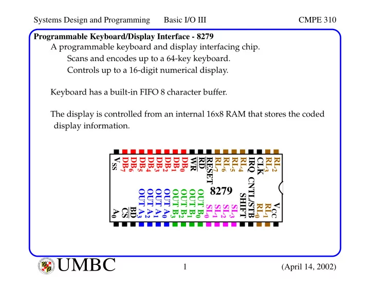
U M B C U N I V E R S I T Y O F M A R Y L A N D B A L T I M O R E C O U N T Y 1 9 6 6Programmable Keyboard/Display Interface - 8279 A programmable keyboard and display interfacing chip. Scans and encodes up to a 64-key keyboard. Controls up to a 16-digit numerical display. Keyboard has a built-in FIFO 8 character buffer. The display is controlled from an internal 16x8 RAM that stores the coded display information.
8279
A0 CS BD OUT A3 OUT A2 OUT A1 OUT A0 OUT B3 OUT B2 OUT B1 OUT B0 SL0 SL1 SL2 SL3 SHIFT CNTL/STB RL0 RL1 VCC VSS DB7 DB6 RESET RL7 RL6 RL5 RL4 IRQ CLK RL3 RL2 DB0 WR RD DB1 DB2 DB3 DB4 DB5