
SLIDE 1
Advanced VLSI Design Details of the MOS Transistor III CMPE 640 1 (10/12/04)
UMBC
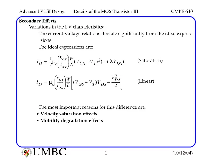
U M B C U N I V E R S I T Y O F M A R Y L A N D B A L T I M O R E C O U N T Y 1 9 6 6Secondary Effects Variations in the I-V characteristics: The current-voltage relations deviate significantly from the ideal expres- sions. The ideal expressions are: The most important reasons for this difference are:
- Velocity saturation effects
- Mobility degradation effects
ID 1 2
- µn
εox tox
-
W L
- VGS
VT – ( )2 1 λVDS + ( ) = ID µn εox tox
-
W L
- VGS
VT – ( )VDS VDS
2
2
- –
= (Saturation) (Linear)