
SLIDE 1
Advanced VLSI Design CMOS Processing Technology II CMPE 640 1 (9/27/04)
UMBC
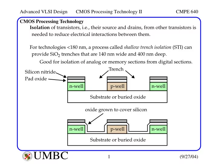
U M B C U N I V E R S I T Y O F M A R Y L A N D B A L T I M O R E C O U N T Y 1 9 6 6CMOS Processing Technology Isolation of transistors, i.e., their source and drains, from other transistors is needed to reduce electrical interactions between them. For technologies <180 nm, a process called shallow trench isolation (STI) can provide SiO2 trenches that are 140 nm wide and 400 nm deep. Good for isolation of analog or memory sections from digital sections. Substrate or buried oxide p-well n-well n-well Pad oxide Silicon nitride Trench Substrate or buried oxide p-well n-well n-well
- xide grown to cover silicon