UMBC A B M A L T F O U M B C I M Y O R T 1 (May - - PowerPoint PPT Presentation

umbc
SMART_READER_LITE
LIVE PREVIEW

UMBC A B M A L T F O U M B C I M Y O R T 1 (May - - PowerPoint PPT Presentation

Systems Design and Programming DMA I CMPE 310 Disk Memory Systems Magnetic and optical: Floppy disks Hard disks CD-ROMs and WORMs (write once/read mostly) DVD Floppy: Sector Outter track Commonly hold between 512 to


slide-1
SLIDE 1

Systems Design and Programming DMA I CMPE 310 1 (May 5, 2002)

UMBC

U M B C U N I V E R S I T Y O F M A R Y L A N D B A L T I M O R E C O U N T Y 1 9 6 6

Disk Memory Systems Magnetic and optical:

  • Floppy disks
  • Hard disks
  • CD-ROMs and WORMs (write once/read mostly)
  • DVD

Floppy: Inner track Outter track Sector Commonly hold between 512 to 1024 bytes of data.

slide-2
SLIDE 2

Systems Design and Programming DMA I CMPE 310 2 (May 5, 2002)

UMBC

U M B C U N I V E R S I T Y O F M A R Y L A N D B A L T I M O R E C O U N T Y 1 9 6 6

Floppy Older 5 and 1/4 flexable floppies spin at 300 RPM, have 40 tracks with 9 sec- tors/track and two sides. Capacity = 40 X 2 X 9 X 512 = 368,640 or ~360K bytes of information. Newer ones are high-density with 80 tracks and 15 sector/track for 1.2 MB. Heads actually contact the disk surface, leading to wear out. The recording format called MFM (modified frequency modulation) used to write double density format. D C D C D C D C D C D C D C 1 1 1 1

slide-3
SLIDE 3

Systems Design and Programming DMA I CMPE 310 3 (May 5, 2002)

UMBC

U M B C U N I V E R S I T Y O F M A R Y L A N D B A L T I M O R E C O U N T Y 1 9 6 6

Floppy The rules are given as follows: A data pulse is always stored for a logic 1. No data and no clock is stored for the first logic 0 in a string of logic 0s. The second and subsequent logic 0s in a row contain a clock pulse, but no data pulse. The clock is inserted in subsequent 0s to maintain synchronization as data is read from the disk. The micro-fl

  • ppy is much mor e popular today:

Head slot Head door Write protect

slide-4
SLIDE 4

Systems Design and Programming DMA I CMPE 310 4 (May 5, 2002)

UMBC

U M B C U N I V E R S I T Y O F M A R Y L A N D B A L T I M O R E C O U N T Y 1 9 6 6

Floppy Advantages of the micro-fl

  • ppy over the mini-fl
  • ppy .

Rigid plastic case provided better protection. Head door kept disk from being exposed. Write protection mechanism. Keyed mechansim for track 0. Increase in storage capacity: 80 tracks X 2 sides X 18 sectors/track X 512 bytes/sector = 1.44 MB. Extended high density micro-fl

  • ppy capable of 2.88 MB.

A second extension is the fl

  • ptical disk which stores data magnetically using

an optical tracking system. It stores 21 MB of data. Hard Disks: Use a fl ying head to stor e and read data from the platters and spins at 3,000 to 10,000 RPM (> 10X that of fl

  • ppies).
slide-5
SLIDE 5

Systems Design and Programming DMA I CMPE 310 5 (May 5, 2002)

UMBC

U M B C U N I V E R S I T Y O F M A R Y L A N D B A L T I M O R E C O U N T Y 1 9 6 6

Hard Disks Hard disks usually have at least 4 platters and can have 2 heads per surface. The heads are moved from cylinder to cylinder using a voice coil. Hard disks use MFM or RLL (run-length limited) to store information. RLL 2,7 is common today -- this indicates that the number of zeros in a row is always between 2 and 7. platter surface head track sector cylinder Stepper motor or voice coil

slide-6
SLIDE 6

Systems Design and Programming DMA I CMPE 310 6 (May 5, 2002)

UMBC

U M B C U N I V E R S I T Y O F M A R Y L A N D B A L T I M O R E C O U N T Y 1 9 6 6

Hard Disks The data is first encoded using the table given below. Note that this encoding always guarantees at least 2 zeros and no more than 7 zeros in a row. This encoding allows nearly a 50% increase in storage capacity over MFMs without changing the driver electronics or disk surface. RLL drives increase the number of tracks from 18 to 27 to achieve this. 40 MB -> 60 MB with better performance.

Input Data Stream RLL output 000 000100 10 0100 010 100100 0010 00100100 11 1000 011 001000 0011 00001000

slide-7
SLIDE 7

Systems Design and Programming DMA I CMPE 310 7 (May 5, 2002)

UMBC

U M B C U N I V E R S I T Y O F M A R Y L A N D B A L T I M O R E C O U N T Y 1 9 6 6

Hard Disks For example, given the data stream 101001011: Although all disks use MFM or RLL, disk interfaces vary. Todays systems use ESDI (non-existent), SCSI (small computer system interface) and IDE (integrated drive electronics). IDE incorporates the disk controller in the disk drive and usually contain a 32 KB cache. Access times are less than 10ms (compared with 200ms for fl

  • ppies).

1 1 1 1 1 MFM RLL 010 001 001 001 001 000

slide-8
SLIDE 8

Systems Design and Programming DMA I CMPE 310 8 (May 5, 2002)

UMBC

U M B C U N I V E R S I T Y O F M A R Y L A N D B A L T I M O R E C O U N T Y 1 9 6 6

Optical Disks CD-ROMs and WORMs store up to 660 MB of data. DVDs are similar but have much higher bit density (4.7, 8.5 and 17 GB). land pit Laser Photodiode Lenses Lenses Transparent, protective layer CD-ROM

slide-9
SLIDE 9

Systems Design and Programming DMA I CMPE 310 9 (May 5, 2002)

UMBC

U M B C U N I V E R S I T Y O F M A R Y L A N D B A L T I M O R E C O U N T Y 1 9 6 6

Video Displays Color displays are extremely popular. Some accept informaton as a composite video signal (similar to TVs), as TTL voltage level signals (0 or 5V) and as analog signals (0 to 0.7V). Composites are disappearing since high-resolution cannot be achieved. They combine the color information with other information such as sync pulses. Most modern systems use direct vido signals with separate sync signals. Monochrome monitors use one wire for video, one for horizontal sync and one for vertical sync. Color monitors use three video signals, one for red, green and blue (RGB). The TTL RGB Monitor: It uses TTL level signs (0 or 5V) as video inputs and a 4th line called intensity. It can display a total of 16 different colors (CGA in older systems).

slide-10
SLIDE 10

Systems Design and Programming DMA I CMPE 310 10 (May 5, 2002)

UMBC

U M B C U N I V E R S I T Y O F M A R Y L A N D B A L T I M O R E C O U N T Y 1 9 6 6

TTL RGB Monitor The following table gives the RGB values and colors: Cyan is a combination of Green and Blue, Magenta - Red and Blue, etc.

Intensity Red Green Blue Color Black 1 Blue 1 Green 1 1 Cyan 1 Red 1 1 Magenta 1 1 Brown 1 1 1 White 1 Gray 1 1 Bright Blue 1 1 Bright Green 1 1 1 Bright Cyan 1 1 Bright Red 1 1 1 Bright Magenta 1 1 1 Yellow 1 1 1 1 Bright White

slide-11
SLIDE 11

Systems Design and Programming DMA I CMPE 310 11 (May 5, 2002)

UMBC

U M B C U N I V E R S I T Y O F M A R Y L A N D B A L T I M O R E C O U N T Y 1 9 6 6

TTL and Analog RGB Monitor The connector pin definitions for either color or monochrome Horizontal and vertical retrace are for synchronization. Normal video is used for “intensity” on monochrome monitors. Analog RGB Monitors Analog RGB monitors have 3 video signals (no intensity) that can be driven with values between 0 and 0.7 V. Most can display 256K, 16M or 24M colors. 59 4 8 3 2 1 7 6 1 and 2: Ground 3: Red video 4: Green video 5: Blue video 6: Intensity 7: Normal video 8: Horizontal retrace 9: Vertical retrace 8157146 5 4 13 12 1: Red 2: Green (mono) 3: Blue 4 and 5: GND 9: Female is blocked 10 and 15: GND 11: Color detect (GND mono) 3 11 2 10 1 9 6/7/8: RGB GND 12: Mono detect (GND color) 13: Horz sync 14: Vert sync 15: GND

slide-12
SLIDE 12

Systems Design and Programming DMA I CMPE 310 12 (May 5, 2002)

UMBC

U M B C U N I V E R S I T Y O F M A R Y L A N D B A L T I M O R E C O U N T Y 1 9 6 6

Analog RGB Monitor Most analog displays use a DAC to generate each color video voltage. A common standard uses a 6-bit DAC for each video signal for 64 dis- tinct voltage levels over 0 to 0.7 V range. 64 X 64 X 64 = 262,144 (256K) colors. 8-bit DACs yield 16M colors. Conversion time between 25ns and 40ns is required of the DAC. The next slide shows the video generation circuit used in VGA systems. Each color is generated with a 18-bit digital code (6 each for RG &B). A high speed palette SRAM (access < 40ns) is used to store 256 different 18-bit color codes (hardware colormap) out of the 256K possible (218). The 8-bit values (8 bit depth) in the video display RAM specify one of the 256 colors for each pixel position on the screen.

slide-13
SLIDE 13

Systems Design and Programming DMA I CMPE 310 13 (May 5, 2002)

UMBC

U M B C U N I V E R S I T Y O F M A R Y L A N D B A L T I M O R E C O U N T Y 1 9 6 6

Analog RGB Monitor I1 I2 I3 I4 I5 I6 I7 I8 16R8 O1 O2 O3 O4 O5 O6 O7 O8 RTC S0 S1 S2 WR Clk OE 25 D0 D5 Q0 Q5 OCClk DAC DAC DAC D0 ... ... D0 D5 Q0 Q5 OCClk ... ... D0 D5 Q0 Q5 OCClk ... ... D0 D5 Q0 Q5 OCClk ... ... ... D17 A0 ... A7 CS OE WE 256x18 Palette RAM D0 D5 Q0 Q5 OCClk ... ... D0 D5 Q0 Q5 OCClk ... ... 1A1 2A4 1Y1 2Y4 1G ... ... 18 2G 1A1 2A4 1Y1 2Y4 1G ... ... 2G 1A1 2A4 1Y1 2Y4 1G ... ... 2G 8 6 6 6 MHz

D0 D5 Q0 Q5 OCClk ... ...

VGA circuit U10 U1 U2 U3 U4 U5 U6

slide-14
SLIDE 14

Systems Design and Programming DMA I CMPE 310 14 (May 5, 2002)

UMBC

U M B C U N I V E R S I T Y O F M A R Y L A N D B A L T I M O R E C O U N T Y 1 9 6 6

Analog RGB Monitor The 8 bit values from the video RAM are each sent individually on the data bus and latched into U10 by the 16R8. After 40ns (1/25MHz), the PAL generates a Clk pulse for the DAC latches. This leaves enough time for the SRAM to access the 18-bit code. The DACs then convert the 6-bit values to analog voltages for the monitor. Changing the 18-bit color values is done during retrace, e.g. when RTC is 1. The PAL latches the address into U10 of the 18-bit cell to overwrite. Then, S0, S1 and S2 are used to clock each of U1, U2 and U3 in succession as 6-bit values are placed on the data bus. Finally, WE of the SRAM is pulsed and the U1-U3 outputs are input to the SRAM.

slide-15
SLIDE 15

Systems Design and Programming DMA I CMPE 310 15 (May 5, 2002)

UMBC

U M B C U N I V E R S I T Y O F M A R Y L A N D B A L T I M O R E C O U N T Y 1 9 6 6

Analog RGB Monitor Retrace occurs 70.1 times per second in the vertical direction and 31,500 times per second in the horizontal direction for a 640 x 480 display. During retrace, the video sent to the monitor must be 0 (black). Buffers U4, U5 and U6 are enabled during this time to force 0. ... 70.1 Hz 31,500 Hz Monitor Video

slide-16
SLIDE 16

Systems Design and Programming DMA I CMPE 310 16 (May 5, 2002)

UMBC

U M B C U N I V E R S I T Y O F M A R Y L A N D B A L T I M O R E C O U N T Y 1 9 6 6

Analog RGB Monitor The resolution of the display determine the amount of memory required. If 256 colors are used (8-bits per pixel) then 640 (width) x 480 or 307,200 bytes of memory are required to store the image. In order to repaint the 640 pixels of a raster line, 40ns X 640 or 25.6 us are needed. A horizontal time of 1/31,500 gives 31.746 us. 31.746 - 25.6 = 6.146 us is allowed for horizontal retrace. Given a vertical retrace of 70.1 Hz, the number of lines repainted is given by (1/70.1)/31.746 us = 449.358 lines. Assume 400 of these lines are used to display information and the rest are lost during retrace. This leaves 49.358 X 31.746 = 1567 us for vertical retrace. It is during this time that the palette can be updated or the display RAM is updated with a new image.

slide-17
SLIDE 17

Systems Design and Programming DMA I CMPE 310 17 (May 5, 2002)

UMBC

U M B C U N I V E R S I T Y O F M A R Y L A N D B A L T I M O R E C O U N T Y 1 9 6 6

Direct Memory Access (DMA) An alternative to the basic and interrupt-driven I/O discussed previously. DMA allows data to be transferred between memory and the I/O device without processor intervention. Speed of transfer limited to speed of memory components or DMA controller (up to 32-40 Mbytes/sec). Common DMA operations: DRAM refresh Video refresh Disk-memory system reads and writes. Two signals are used to request/ack a DMA transfer: HOLD is an input to the micro that requests a DMA action. HLDA is an output from the micro granting the DMA action. The microprocessor responds by suspending the execution of the program and by placing its address, data and control bus in high-impedance states.

slide-18
SLIDE 18

Systems Design and Programming DMA I CMPE 310 18 (May 5, 2002)

UMBC

U M B C U N I V E R S I T Y O F M A R Y L A N D B A L T I M O R E C O U N T Y 1 9 6 6

Direct Memory Access (DMA) DMA “reads” refer to transfers from memory to an I/O device and involves the use of MRDC and IOWC. DMA “writes” refer to transfers from an I/O device to memory and involves the use of MWTC and IORC. The data transfer rate is determined by the speed of memory or the DMA controller (usually the latter). The DMA controller provides memory with the address and select the appro- priate I/O device (via DACK).

8239

DB7 DB6 DB5 DACK1 DACK0 DB4 DB3 DB2 DB1 DB0 A0 A1 A2 A3 EOP A4 A5 A6 A7 VSS DREQ0 DREQ1 AEN ADSTB HLDA READY MEMW MEMR IOW IOR CLK CS HRQ RESET DACK2 DACK3 DREQ3 DREQ2 VCC x

slide-19
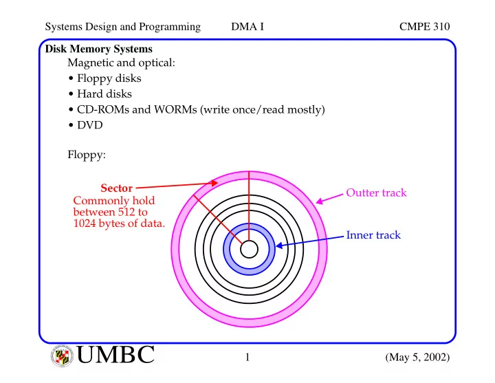
SLIDE 19

Systems Design and Programming DMA I CMPE 310 19 (May 5, 2002)

UMBC

U M B C U N I V E R S I T Y O F M A R Y L A N D B A L T I M O R E C O U N T Y 1 9 6 6

8237 Clk: < 5MHz. CS: Output of a decoder. RESET: Clears all internal registers (command, status, request, etc). READY: Allows memory and I/O to insert wait states into the 8237. HLDA: Input that tells 8237 that micro has released address, data and con- trol buses. DREQ3-DREQ0: DMA request inputs used to request a DMA transfer. DB7-DB0: Used to program the 8237 and output upper 8-bits of address. IOR, IOW, MEMR, MEMW: Outputs used to control memory and I/O. EOP: Bidirectional: as an input, used to terminate a DMA transfer, as an

  • utput, signals the end of the DMA transfer.

A3-A0: Address pins select an internal register during programming and

  • utput part of the address for a transfer.

A7-A4: Address outputs. HRQ: Output that connects to HOLD pin on micro to request a DMA. DACK3 - DACK0: Used to select an I/O device (ack a DMA request). AEN/ADSTB: Enable latch (and strobe) to transfer DBx to upper 8 A bits.

slide-20
SLIDE 20

Systems Design and Programming DMA I CMPE 310 20 (May 5, 2002)

UMBC

U M B C U N I V E R S I T Y O F M A R Y L A N D B A L T I M O R E C O U N T Y 1 9 6 6

8237 Some of the internal registers are: CAR3 - CAR0: Used to hold the 16-bit memory address used for a DMA

  • transfer. Either incremented or decremented after a byte is transferred.

CWCR3 - CWCR0: Current word count register programs a channel for the # of bytes (up to 64KB) transferred during a DMA action. CR: Command register programs the operation of the 8237. Bits in this reg- ister allow: Memory-to-memory transfers (like MOVSB) where DMA channel 0 holds the source address and DMA channel 1 holds the dest address. Memory-to-memory transfers in which DMA channel 0 holds a constant address -- used to fill a memory regions with a constant. Fixed or rotating DMA channel priority, plus misc other options. MR: “ Mode of operation” r egister -- one for each channel. For example, block mode is used for memory-to-memory transfers. RR: Request register is used to request a DMA transfer via software -- essential for processor initiated memory-to-memory transfers. SR: Status register indicates when a DMA has completed.

slide-21
SLIDE 21

Systems Design and Programming DMA I CMPE 310 21 (May 5, 2002)

UMBC

U M B C U N I V E R S I T Y O F M A R Y L A N D B A L T I M O R E C O U N T Y 1 9 6 6

DMA-Processed Printer Interface Note that the I/O device is NOT selected by decoding the address bus, but rather by DACK, since address bus contains a memory address. See code in book and example of 8237 connected to an 8088. (pp. 506). 8239

IORC ‘373 G OE

Data to Printer D7 D0 J K DACK3 DREQ3 Q Set Clear ‘122 DS Clk ACK TR Q Q Latch DACK3 latches data in ‘373 and generates DS to printer through the single shot ‘122. ACK indicates printer needs data -- also used as a DMA request. Once programmed with address of data and # of chars, the 8239 transfers a byte at a time.