UMBC A B M A L T F O U M B C I M Y O R T 1 - - PowerPoint PPT Presentation

umbc
SMART_READER_LITE
LIVE PREVIEW

UMBC A B M A L T F O U M B C I M Y O R T 1 - - PowerPoint PPT Presentation

Digital Systems Terminations I CMPE 650 Terminations From our previous analysis, a cable needs to be terminated when Its long (its length exceeds 1/6 the electrical length of the rising edge) and reflections occur Its short (its


slide-1
SLIDE 1

Digital Systems Terminations I CMPE 650 1 (4/17/07)

UMBC

U M B C U N I V E R S I T Y O F M A R Y L A N D B A L T I M O R E C O U N T Y 1 9 6 6

Terminations From our previous analysis, a cable needs to be terminated when

  • It’s long (its length exceeds 1/6 the electrical length of the rising edge) and

reflections occur

  • It’s short (its has large inductance and drives a large capacitive load) and

ringing occurs Resistive terminations can cure both of these problems. There are two main types:

  • End terminations
  • Series terminations

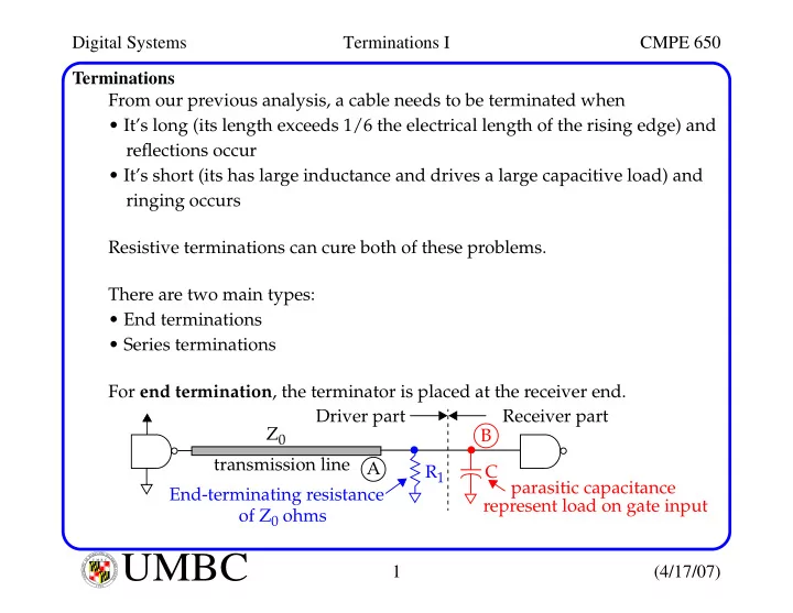
For end termination, the terminator is placed at the receiver end. Z0 transmission line A R1 B C parasitic capacitance represent load on gate input End-terminating resistance

  • f Z0 ohms

Driver part Receiver part

slide-2
SLIDE 2

Digital Systems Terminations I CMPE 650 2 (4/17/07)

UMBC

U M B C U N I V E R S I T Y O F M A R Y L A N D B A L T I M O R E C O U N T Y 1 9 6 6

End Terminations Characteristics:

  • The driving wfm propagates at full intensity all the way down the cable
  • All reflections are damped by the terminating resistor
  • The received voltage is equal to the transmitted voltage

Rise time: The Thevenin equivalent driving impedance is the transmission line impedance Z0, in parallel with the terminating resistor (also Z0). This yields a drive impedance (for short term events) of Z0/2. The receiving part consists of a load capacitor (a good model for CMOS, TTL or ECL). Therefore, this RC filter has a time constant: τ Z0 2

  • C

= previously we formulated T10-90 2.2 Z0 2

  • C

1.1Z0C = =

slide-3
SLIDE 3

Digital Systems Terminations I CMPE 650 3 (4/17/07)

UMBC

U M B C U N I V E R S I T Y O F M A R Y L A N D B A L T I M O R E C O U N T Y 1 9 6 6

End Terminations The point B rise time is then computed from the "averaging method": This is a good model if the line is long. When it is short (i.e., comparable to the length of its rising edge), the imped- ance as seen at B goes down. In the limit, the driving impedance is just the output impedance of the driver. This gives a faster rise time at point B. See the text for a derivation using our previous model for a transmission line: An end-terminated capacitively coupled rise time is half that of a series termi- nated line (described below) under the same load conditions. TB T10-90

2

T1

2

+ = T1 is the incoming signal rise time S∞ ω ( ) A ω ( )Hx ω ( ) R2 ω ( ) 1 + ( ) 1 R2 ω ( )Hx

2 ω

( )R1 ω ( ) –

  • =
slide-4
SLIDE 4

Digital Systems Terminations I CMPE 650 4 (4/17/07)

UMBC

U M B C U N I V E R S I T Y O F M A R Y L A N D B A L T I M O R E C O U N T Y 1 9 6 6

End Terminations The termination arrangement just discussed rarely appears in TTL or CMOS circuits because of the large drive current to maintain a high state. The driver must supply VCC/R1 to the terminating resistor. With Z0 equal to 65-Ω, a 5-V signal requires 5/65 = 76mA! Alternatively, one can use a split termination: Here, the ratio R1/R2 controls the relative proportion of high vs low current. This type of termination is sometimes used to terminate ECL circuits. Z0 transmission line A R2 B C parasitic capacitance represent load on gate input R1||R2 is Z0 ohms Driver part Receiver part R1

slide-5
SLIDE 5

Digital Systems Terminations I CMPE 650 5 (4/17/07)

UMBC

U M B C U N I V E R S I T Y O F M A R Y L A N D B A L T I M O R E C O U N T Y 1 9 6 6

End Terminations Setting R1 = R2 equalizes the current requirements for use with HCMOS. If R2 > R1, low current exceeds high current, appropriate for TTL and HCT. The selection of R1 and R2 can be done graphically under 3 constraints:

  • The parallel combination must equal Z0.
  • We must not exceed IOHmax (max high-level output current) or IOLmax.

Assume sink current (entering the driver) is positive and source current is negative. TTL and CMOS sinks current in low state and sources current in high state while ECL sources current in both states. In order to keep our constraint equations linear, we use admittances: Y1 1 R1

  • =

Y2 1 R2

  • =

Y1 Y2 + 1 Z0

  • =

&

slide-6
SLIDE 6

Digital Systems Terminations I CMPE 650 6 (4/17/07)

UMBC

U M B C U N I V E R S I T Y O F M A R Y L A N D B A L T I M O R E C O U N T Y 1 9 6 6

End Terminations This constraint can be graphed: All valid combinations of Y1 and Y2 lie on the green and blue lines for a given Z0. The equations for the two other constraints is derived by noting the current that flows in the driver equals the current flowing in R2 minus R1. R2 R1 5V Idriver 5.5V Y1 Y2 0.01 0.02 0.01 0.02 100 Ω constraint line IOH constraint: 0.7Y1 - 4.8Y2 > -0.024 IOL constraint: 5.06Y1 - 0.44Y2 < 0.024 Region satisfying both constraints 74HC11000 NAND gate analysis 65 Ω Sum of constants is 5.5V. Difference gives current through driver

slide-7
SLIDE 7

Digital Systems Terminations I CMPE 650 7 (4/17/07)

UMBC

U M B C U N I V E R S I T Y O F M A R Y L A N D B A L T I M O R E C O U N T Y 1 9 6 6

End Terminations These currents depend on VCC, VEE and the driver output voltage. Note the left and right members of IOHmax equation are negative numbers. Also, the value of IOLmax is a positive number for TTL and CMOS but is zero for ECL. The 100-Ω line shown in the graph passes the constraint line limits and yields resistance values for R1 and R2 of 200 Ω. On the other hand, the 65-Ω line does not satisfy both current constraints at any point, and therefore cannot drive a 65-Ω load. VCC VOH – ( )Y1 VOH VEE – ( )Y2 – IOHmax > VCC VOL – ( )Y1 VOL VEE – ( )Y2 – IOLmax < high output state low output state

slide-8
SLIDE 8

Digital Systems Terminations I CMPE 650 8 (4/17/07)

UMBC

U M B C U N I V E R S I T Y O F M A R Y L A N D B A L T I M O R E C O U N T Y 1 9 6 6

Other Topologies Used with End Terminations The bifurcated line cannot be terminated properly since signal energy will always refl ects of f the junction at point A, causing ringing. However, the following configuration can be properly terminated: 5V Z0 Z0 A Z0 5V 2Z0 2Z0 A Z0 R1 = 2Z0 R2 = 2Z0 These lines are skinner than main feed Not often used because of the difficulty to fabricate

slide-9
SLIDE 9

Digital Systems Terminations I CMPE 650 9 (4/17/07)

UMBC

U M B C U N I V E R S I T Y O F M A R Y L A N D B A L T I M O R E C O U N T Y 1 9 6 6

Other Topologies Used with End Terminations End termination allows receivers to be placed at any point along the line. Each receiver sees a delayed version of the signal. Keep the connecting stubs short compared to the length of the rising edge to avoid refl ections at the bifur cation points. 5V Main path Daisy chain configuration Each adds a capacitive load that degrades rise time Right way Wrong way Driver From Driver From

slide-10
SLIDE 10

Digital Systems Terminations I CMPE 650 10 (4/17/07)

UMBC

U M B C U N I V E R S I T Y O F M A R Y L A N D B A L T I M O R E C O U N T Y 1 9 6 6

Power Dissipation in End Terminators Load dissipation is inversely proportional to the terminating impedance and

  • bviously depends on the high and low operating voltages.

Under the assumption that equal amounts of time are spent in the high and low states, the power dissipated in the load resistors is given by: The power dissipated in the driving circuit was discussed previously. Source Terminators This scheme connects the driver to the impedance line through a resistor. The sum of the driver source impedance plus this resistor should equal Z0 (the characteristic impedance of the transmission line). Under these conditions, the refl ection coef ficient at the src is zero. Pload VHI VEE – ( )2 VLO VEE – ( )2 + 2R2

  • VCC

VHI – ( )2 VCC VLO – ( )2 + 2R1

  • +

=

slide-11
SLIDE 11

Digital Systems Terminations I CMPE 650 11 (4/17/07)

UMBC

U M B C U N I V E R S I T Y O F M A R Y L A N D B A L T I M O R E C O U N T Y 1 9 6 6

Source Terminators Source terminated circuits have several properties:

  • The drive wfm is cut in half before it begins propagating down the line.
  • The driving signal propagates at 1/2 intensity to the end of the line.
  • At the far end, the signal refl ection is +1 (for an open cir

cuit). From previous discussions, the refl ecting half intensity signal in combi- nation with the incoming half intensity signal restore the signal.

  • The refl ected signal pr
  • pagates back and damps out at the source termina-

tion (drive current becomes zero at this point). R1 = Z0 A B C D Propagation delay T seconds Z0 T 2T 1/2 1 1/2 1 1

slide-12
SLIDE 12

Digital Systems Terminations I CMPE 650 12 (4/17/07)

UMBC

U M B C U N I V E R S I T Y O F M A R Y L A N D B A L T I M O R E C O U N T Y 1 9 6 6

Resistance Value of Source Termination "Real" drivers have a small resistive output impedance (ECL is ~ 10Ω in either the high or low state). Given the driver impedance + source terminating resistor = Z0, the source terminating resistance is typically smaller than the line impedance. TTL and CMOS have different output impedances in their high and low states. Therefore, the source terminating resistance is a compromise. From any point along the line, looking back, the drive impedance is Z0. For capacitive loads, we get a simple RC low-pass filter with time constant Therefore, the rise time is twice as long as the rise time of an end-terminated with the same transmission line impedance and load. RC time constant Z0C = yielding a 10-90% rise time T10-90 2.2Z0C =

slide-13
SLIDE 13

Digital Systems Terminations I CMPE 650 13 (4/17/07)

UMBC

U M B C U N I V E R S I T Y O F M A R Y L A N D B A L T I M O R E C O U N T Y 1 9 6 6

Flatter Step Response of Source Termination It is easier to eliminate refl ections at the sour ce than at the far end of a trans- mission line in digital circuits. While the src has a resistive output load (plus a little inductance), the receiver usually has a capacitive load which is usually more difficult to match. This is especially true when driving multiple loads. Therefore, the reflection coefficient at the driver is more nearly zero than the coefficient at the receiver under end-termination. This gives a fl atter overall fr equency response. Drive Current Requirements: The composite input impedance of a src-terminated line includes both Z0 and the src-termination resistor -- sum is nearly 2*Z0. The worst case drive current is: ∆V 2Z0 ⁄

slide-14
SLIDE 14

Digital Systems Terminations I CMPE 650 14 (4/17/07)

UMBC

U M B C U N I V E R S I T Y O F M A R Y L A N D B A L T I M O R E C O U N T Y 1 9 6 6

Drive Current Requirements by Source Termination This worst case drive current lasts only as long as the round-trip delay. End-terminated transmission lines require exactly the same maximum drive current if the end terminator is biased halfway between the logic levels. Thus they are no more difficult to drive the src-terminated lines. The input impedance of an end-terminated line is Z0 (half that of a src-termi- nated line). However, the maximum voltage difference between logic high or low and the halfway bias point is ∆V/2, yielding a current: Note that for end-terminations, adjustment of the bias point allows adjust- ment of the magnitude of the high and low current drive. For src-terminations, both polarities take the same amount of current. ∆V 2Z0 ⁄

slide-15
SLIDE 15

Digital Systems Terminations I CMPE 650 15 (4/17/07)

UMBC

U M B C U N I V E R S I T Y O F M A R Y L A N D B A L T I M O R E C O U N T Y 1 9 6 6

Other Topologies and Power Dissipation of Source Terminators The daisy-chain topology does not work with src-terminators. All loads must connect to the end of the line. Loads connected midway will see the C wfm shown in the previous fig. Power Dissipation (generally less than power used in end-terminated load): The src-termination resistor has a voltage of ∆V/2 impressed across it during the entire round trip delay 2T after switching. During this time, the src-terminating resistor dissipates a total energy of: In the case that the pulse rate is greater than 2T, multiply this energy/pulse times the pulse rate to get the power dissipation. Otherwise, assume that ∆V/2 is across the resistor at all times: E 2T ∆V 2

   21 R

  • =

∆V is the difference between high and low Power pulse freq ( )T∆V2 2R

  • =
slide-16
SLIDE 16

Digital Systems Terminations I CMPE 650 16 (4/17/07)

UMBC

U M B C U N I V E R S I T Y O F M A R Y L A N D B A L T I M O R E C O U N T Y 1 9 6 6

Middle Terminators Systems with large fanouts and tristate drivers (a hair-ball) can result in a large amount of ringing. The rattling lasts at least as long as the longest contiguous length in the hair- ball. If devices in the network require monotonically rising edges, the only fix is to slow down the rising edges or filtering the received signal. If the signal is sampled, the sampling event can be staggered to avoid the ringing. Here, the objective is to reduce the settling time. Four approaches to this problem:

  • Add a src terminator to every driver.
  • Add an end terminator at each receiver.
  • Add a shunt termination in the middle of the network.
  • Add series resistance between every juncture of branches.
slide-17
SLIDE 17

Digital Systems Terminations I CMPE 650 17 (4/17/07)

UMBC

U M B C U N I V E R S I T Y O F M A R Y L A N D B A L T I M O R E C O U N T Y 1 9 6 6

Middle Terminators Option 1 takes little power, provides a little bit of damping and reduces set- tling time. Option 2 requires a lot of drive power but works well in star configurations. A star has a discrete wire leading from each driver and receiver to a cen- tral point. Refl ectionsare confined to the segment between the src and the common connection. Combining options 1 and 2 wastes more power but works perfectly for star configurations, except that signals are attenuated through the star. Option 3 is stupid -- don’t use it. It lowers the impedance of the central part

  • f the network where it is already too low.

Option 4 attenuates the signal at every juncture.

slide-18
SLIDE 18

Digital Systems Terminations I CMPE 650 18 (4/17/07)

UMBC

U M B C U N I V E R S I T Y O F M A R Y L A N D B A L T I M O R E C O U N T Y 1 9 6 6

Middle Terminators Option 4 (cont): In this configuration, the signal attenuates by 1/2 as it passes through each juncture. This damps out refl ections quickly (r

  • und-trip attenuation is 1/4) but also

cuts down the signal level severely as the signal traverses many of these. Therefore, you’ll need to establish an upper limit on the number of junctures you can tolerate at the receiver. Z0 Z0 Z0 All resistors are Z0/3