
SLIDE 1
Advanced VLSI Design Scaling CMPE 640 1 (10/18/04)
UMBC
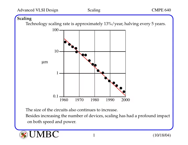
U M B C U N I V E R S I T Y O F M A R Y L A N D B A L T I M O R E C O U N T Y 1 9 6 6Scaling Technology scaling rate is approximately 13%/year, halving every 5 years. The size of the circuits also continues to increase. Besides increasing the number of devices, scaling has had a profound impact
- n both speed and power.
1 0.1 1960 1970 1980 2000 1990 10 100 µm