
SLIDE 1
Digital Systems Power Systems I CMPE 650 1 (5/6/08)
UMBC
U M B C U N I V E R S I T Y O F M A R Y L A N D B A L T I M O R E C O U N T Y 1 9 6 6Power Systems Serve to:
- Provide stable voltage references
- Distribute power to all logic devices
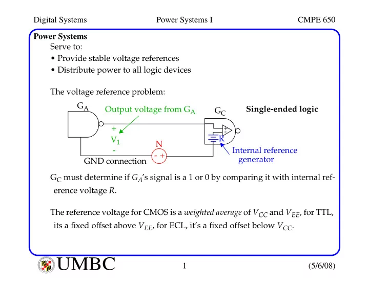
The voltage reference problem: GC must determine if GA’s signal is a 1 or 0 by comparing it with internal ref- erence voltage R. The reference voltage for CMOS is a weighted average of VCC and VEE, for TTL, its a fixed offset above VEE, for ECL, it’s a fixed offset below VCC. GA
+
- Internal reference
generator +
- V1
+
- N
GND connection Output voltage from GA GC Single-ended logic R