
SLIDE 1
Principles of VLSI Design CMOS Processing Technology CMSC 491B/711 1 (November 26, 2000 6:48 pm)
UMBC
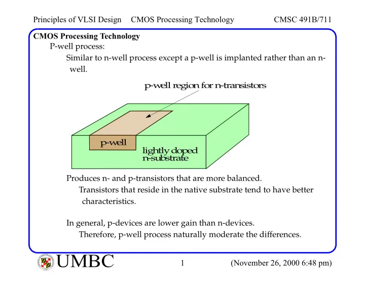
U M B C U N I V E R S I T Y O F M A R Y L A N D B A L T I M O R E C O U N T Y 1 9 6 6CMOS Processing Technology P-well process: Similar to n-well process except a p-well is implanted rather than an n- well. Produces n- and p-transistors that are more balanced. Transistors that reside in the native substrate tend to have better characteristics. In general, p-devices are lower gain than n-devices. Therefore, p-well process naturally moderate the differences.