
SLIDE 1
Advanced VLSI Design Combination Logic Design III CMPE 640 1 (11/29/04)
UMBC
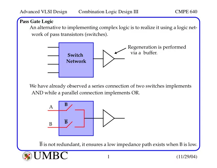
U M B C U N I V E R S I T Y O F M A R Y L A N D B A L T I M O R E C O U N T Y 1 9 6 6Pass Gate Logic An alternative to implementing complex logic is to realize it using a logic net- work of pass transistors (switches). We have already observed a series connection of two switches implements AND while a parallel connection implements OR. B is not redundant, it ensures a low impedance path exists when B is low. Switch Network Regeneration is performed via a buffer. A B B B